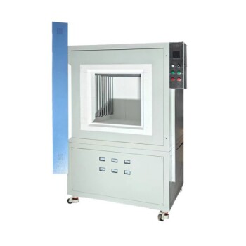
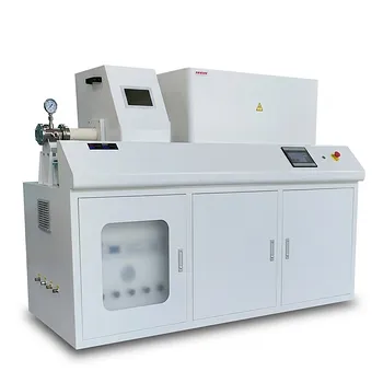
Thermal post-treatment is the critical catalyst for transforming raw Cadmium Sulfide (CdS) depositions into high-performance semiconductor layers. By providing controlled thermal energy, a laboratory oven or annealing furnace facilitates atomic rearrangement, eliminates structural defects, and activates essential chemical dopants. This process ultimately results in superior crystallinity, optimized bandgap properties, and significantly stronger interface bonding within thin-film solar cells.
Core Takeaway: Post-treatment acts as a structural and chemical "reset," transitioning the CdS film from a disordered state to a highly ordered crystalline phase. This optimization is essential for maximizing carrier mobility and ensuring stable heterojunction interfaces in devices like CZTS and bulk heterojunction solar cells.
Enhancing Microstructural Integrity and Crystallinity
Atomic Rearrangement and Stress Relief
The application of heat in an annealing furnace provides the kinetic energy necessary for atoms to migrate to their ideal lattice positions. This atomic rearrangement effectively reduces lattice distortion and internal stresses that are naturally introduced during the initial deposition process.
Eliminating these internal stresses is vital for the long-term physical stability of the thin film. A well-annealed film is less prone to delamination or structural failure when integrated into complex device stacks.
Promoting Recrystallization and Grain Growth
High-temperature environments, often reaching up to 500°C in tube furnaces, induce recrystallization of the CdS film. This process increases the average grain size, which reduces the total area of grain boundaries throughout the material.
Fewer grain boundaries mean fewer obstacles for charge carriers. This improvement in crystalline quality directly leads to higher carrier mobility and better overall efficiency in optoelectronic applications.
Optimizing Optoelectronic Properties
Activation of Dopants and Linking Molecules
In sensitized CdS films, post-treatment at temperatures around 250°C is used to activate internal dopants, such as silver, and linking molecules like Mercaptopropionic acid (MPA). The thermal energy ensures these elements are properly integrated into the film's chemical matrix.
This activation is crucial for tailoring the electrical conductivity of the film. Without this thermal "trigger," the dopants remain dormant, and the film may fail to meet the required electronic specifications.
Bandgap Engineering and Passivation
Annealing allows for the precise adjustment of the bandgap, making the CdS layer more compatible with the light-absorbing layers in a solar cell. Furthermore, when performed with additives like Cadmium Chloride (CdCl2), the furnace drives chlorine elements to the surface to passivate defect states.
Passivation "plugs" the electronic holes at grain boundaries that would otherwise trap electrons. This significantly reduces non-radiative recombination, ensuring more generated current reaches the external circuit.
Interface and Heterojunction Engineering
Improving Bonding Strength and Interface Quality
The quality of the contact between the CdS buffer layer and the subsequent absorber layer (such as CZTS or antimony-based layers) is dictated by the annealing process. Thermal treatment enhances interface bonding strength, creating a more robust mechanical and electrical connection.
A high-quality interface minimizes resistance at the junction. This ensures that the flow of charge between the different semiconductor materials is as efficient as possible.
Atmospheric Control and Phase Transformation
Advanced annealing furnaces allow for precise atmospheric regulation, such as using high-purity argon. This control is essential for preventing unwanted oxidation and can even drive phase transformations from amorphous states to high-performance crystalline phases.
By modulating the environment, engineers can control surface roughness and final optoelectronic properties. This level of precision is what separates experimental lab results from scalable, high-efficiency production.
Understanding Technical Trade-offs and Limitations
The Risk of Over-Annealing
While heat improves crystallinity, excessive temperatures or prolonged exposure can lead to over-annealing. This may cause the film to become too porous or lead to the unwanted diffusion of atoms into adjacent layers, which can degrade the heterojunction.
Thermal Budget Constraints
Every substrate has a thermal budget, or a maximum temperature it can withstand before warping or degrading. Choosing the correct annealing temperature is a delicate balance between optimizing the CdS film and protecting the underlying structural components of the device.
Atmospheric Contamination
If the annealing furnace is not properly sealed or purged, trace amounts of oxygen or moisture can introduce new defects during the heating process. Achieving the benefits of post-treatment requires a high-precision environment to avoid undoing the gains made during deposition.
How to Apply Post-Treatment to Your Project
When designing a post-treatment protocol, your primary goal will dictate your furnace settings and atmospheric requirements.
- If your primary focus is maximizing charge carrier mobility: Prioritize higher temperatures (near 500°C) in a tube furnace to drive recrystallization and significant grain growth.
- If your primary focus is stabilizing a sensitized interface: Focus on lower-temperature treatments (around 250°C) to activate linking molecules and dopants without disturbing the delicate chemical bonds.
- If your primary focus is reducing electronic noise and recombination: Utilize a CdCl2 treatment phase within the furnace to passivate grain boundaries and surface states.
Precision control over the thermal environment is the single most effective way to bridge the gap between a deposited thin film and a high-performance semiconductor device.
Summary Table:
| Improvement Mechanism | Key Technical Action | Resulting Benefit |
|---|---|---|
| Microstructural Integrity | Atomic rearrangement & stress relief | Enhanced physical stability & reduced delamination |
| Crystallinity | Recrystallization & grain growth | Higher carrier mobility due to fewer grain boundaries |
| Optoelectronic Tuning | Dopant & linking molecule activation | Tailored electrical conductivity & efficient charge flow |
| Surface Passivation | Defect state "plugging" (e.g., via CdCl2) | Reduced non-radiative recombination & higher current |
| Interface Quality | Enhanced heterojunction bonding | Lower contact resistance & efficient material junctions |
Ready to achieve superior crystallinity and performance in your semiconductor films? KINTEK specializes in high-precision laboratory equipment designed for rigorous thermal post-treatment. Whether you need tube furnaces for high-temperature recrystallization, vacuum or atmosphere furnaces for precise phase transformation, or CVD/PECVD systems for advanced deposition, our solutions ensure optimal bandgap engineering and interface quality.
We support researchers and industrial labs with a comprehensive portfolio including muffle furnaces, rotary furnaces, high-pressure reactors, and autoclaves, alongside essential consumables like cruibles and ceramics. Empower your thin-film solar cell and battery research today—contact our technical experts now to find the perfect thermal solution for your laboratory!
References
- Asmaa Soheil Najm, Abbas J. Sultan. Towards a promising systematic approach to the synthesis of CZTS solar cells. DOI: 10.1038/s41598-023-42641-w
This article is also based on technical information from Kintek Solution Knowledge Base .
Related Products
- Aluminized Ceramic Evaporation Boat for Thin Film Deposition
- Controlled Nitrogen Inert Hydrogen Atmosphere Furnace
- Graphite Vacuum Furnace High Thermal Conductivity Film Graphitization Furnace
- Multi Heating Zones CVD Tube Furnace Machine Chemical Vapor Deposition Chamber System Equipment
- Electron Beam Evaporation Coating Oxygen-Free Copper Crucible and Evaporation Boat
People Also Ask
- What is the source of evaporation for thin film? Choosing Between Thermal and E-Beam Methods
- Why are high-purity ceramic boats used for lignin activation? Ensure Purity & Thermal Stability
- Why is an alumina boat and Ti3AlC2 powder bed necessary for Ti2AlC sintering? Protect MAX Phase Purity
- Why use an alumina boat for high-temperature carbon activation? Ensure Maximum Material Purity & Thermal Stability
- Why is an alumina boat selected for catalyst precursors? Ensure Sample Purity at 1000 °C