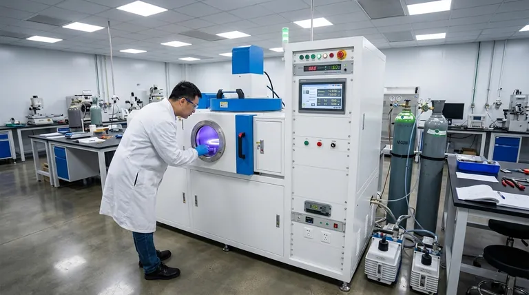
To perform magnetron sputtering, you place a material to be deposited (the target) and a component to be coated (the substrate) into a vacuum chamber. A powerful magnetic field is applied behind the target, and a high voltage is used to ignite a plasma from an inert gas. This plasma bombards the target, ejecting atoms which then travel and deposit onto the substrate, forming a thin, uniform film.
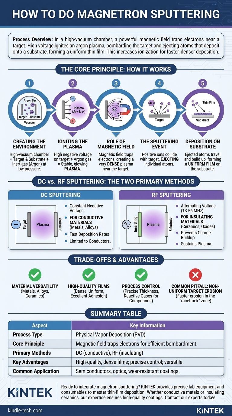
The core concept to grasp is that magnetron sputtering is a highly efficient coating process where a magnetic field is used to trap electrons near the target. This confinement dramatically increases the ionization of gas atoms, leading to a much higher rate of target bombardment and faster, denser film deposition compared to older sputtering methods.
The Core Principle: How Magnetron Sputtering Works
Magnetron sputtering is a type of Physical Vapor Deposition (PVD). The process can be broken down into a few fundamental steps that occur within a high-vacuum environment.
Creating the Environment
First, both the target (the source material you want to deposit) and the substrate (the object you want to coat) are placed inside a vacuum chamber. The chamber is pumped down to a very low pressure to remove contaminants.
An inert gas, most commonly argon, is then introduced into the chamber at a low, controlled pressure.
Igniting the Plasma
A high negative voltage, often several hundred volts, is applied to the target material. This strong electric field pulls free electrons and accelerates them.
These high-energy electrons collide with the neutral argon gas atoms, knocking off their electrons and creating a stable, glowing discharge of positive argon ions and free electrons known as a plasma.
The Role of the Magnetic Field
This is the key step that defines "magnetron" sputtering. A powerful magnetic field is configured behind the target.
This magnetic field traps the highly mobile electrons in a concentrated region close to the target's surface. This dramatically increases the probability that an electron will collide with and ionize an argon atom.
The result is a very dense, stable plasma located precisely where it's needed most—right in front of the target.
The Sputtering Event
The positively charged argon ions in the dense plasma are now strongly attracted to the negatively charged target.
They accelerate towards and collide with the target surface with immense kinetic energy. This bombardment transfers enough energy to knock out, or "sputter," individual atoms from the target material.
Deposition on the Substrate
These ejected atoms from the target travel through the vacuum chamber and land on the substrate.
Over time, these atoms build up layer by layer, forming a thin, uniform, and often very dense film on the substrate's surface.
The Two Primary Methods: DC vs. RF Sputtering
The choice of power supply is the most critical decision in setting up a magnetron sputtering process. It is determined entirely by the electrical properties of your target material.
DC (Direct Current) Sputtering
In DC sputtering, a constant negative voltage is applied to the target. This method is highly efficient and provides fast deposition rates.
Its use is limited to electrically conductive materials, such as metals and transparent conductive oxides. If used with an insulating material, positive charge would build up on the target surface, neutralizing the negative bias and quickly stopping the sputtering process.
RF (Radio Frequency) Sputtering
RF sputtering uses an alternating power supply that rapidly switches the voltage between positive and negative, typically at a frequency of 13.56 MHz.
During the positive cycle, the target attracts electrons, which neutralize the positive ion charge that accumulated during the negative cycle. This prevents charge buildup, making it possible to sputter electrically insulating (dielectric) materials like ceramics, quartz, or oxides.
Understanding the Trade-offs and Advantages
While incredibly versatile, magnetron sputtering has specific characteristics that make it suitable for certain applications over others.
Advantage: Material Versatility
A primary strength of sputtering is its ability to deposit a vast range of materials. Metals, alloys, and even ceramic compounds can be made into targets and deposited effectively.
Advantage: High-Quality Films
The high kinetic energy of the sputtered atoms results in films that are typically very dense, uniform, and have excellent adhesion to the substrate. The atoms can even slightly penetrate the substrate surface, creating a strong bond.
Advantage: Process Control
Engineers have precise control over film thickness down to the angstrom level. Furthermore, by introducing reactive gases (like oxygen or nitrogen) into the chamber, one can form compound films, such as titanium nitride or aluminum oxide, directly on the substrate.
Common Pitfall: Non-Uniform Target Erosion
The magnetic field that makes the process efficient also causes a common issue. The plasma is concentrated in a specific ring-shaped area on the target, known as the "racetrack."
This leads to the target material eroding much faster in this zone, which can affect the long-term stability of the deposition rate and limit the total amount of material that can be used from a single target.
Making the Right Choice for Your Application
Selecting the correct sputtering method is essential for achieving your desired outcome. Your decision should be based directly on the material you intend to deposit.
- If your primary focus is depositing conductive materials (like most metals and alloys): DC magnetron sputtering is the most efficient and cost-effective choice, offering the highest deposition rates.
- If your primary focus is depositing insulating or dielectric materials (like ceramics, SiO₂, or Al₂O₃): RF magnetron sputtering is necessary to prevent charge accumulation on the target surface and sustain the plasma.
- If your primary focus is creating complex compound films (like nitrides or oxides): You will use reactive sputtering, choosing either a DC or RF power supply based on whether your base target material is conductive or insulating.
By understanding these core principles and distinctions, you can effectively leverage magnetron sputtering to engineer surfaces with precisely controlled properties for your project.
Summary Table:
| Aspect | Key Information |
|---|---|
| Process Type | Physical Vapor Deposition (PVD) |
| Core Principle | Magnetic field traps electrons to create dense plasma for efficient target bombardment. |
| Primary Methods | DC Sputtering (conductive materials), RF Sputtering (insulating materials) |
| Key Advantages | High-quality, dense films; excellent adhesion; precise thickness control; material versatility. |
| Common Application | Deposition of metals, alloys, and ceramics for semiconductors, optics, and wear-resistant coatings. |
Ready to integrate magnetron sputtering into your lab's capabilities?
KINTEK specializes in providing the precise lab equipment and consumables you need to master thin-film deposition. Whether you are working with conductive metals or insulating ceramics, our expertise ensures you achieve the high-quality, uniform coatings critical for your research and development.
Contact our experts today via our Contact Form to discuss your specific application and discover how KINTEK's solutions can enhance your laboratory's efficiency and results.
Visual Guide
Related Products
- Spark Plasma Sintering Furnace SPS Furnace
- RF PECVD System Radio Frequency Plasma-Enhanced Chemical Vapor Deposition RF PECVD
People Also Ask
- What is SPS sintering method? A Guide to High-Speed, High-Performance Material Fabrication
- What is the pressure for spark plasma sintering? A Guide to Optimizing SPS Parameters
- What technical advantages does a Spark Plasma Sintering (SPS) furnace offer for LZP ceramics? Enhance Ionic Conductivity
- What are the fundamentals of spark plasma sintering process? Unlock Rapid, High-Performance Material Consolidation
- What is the theory of spark plasma sintering? A Guide to Rapid, Low-Temperature Densification

