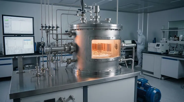
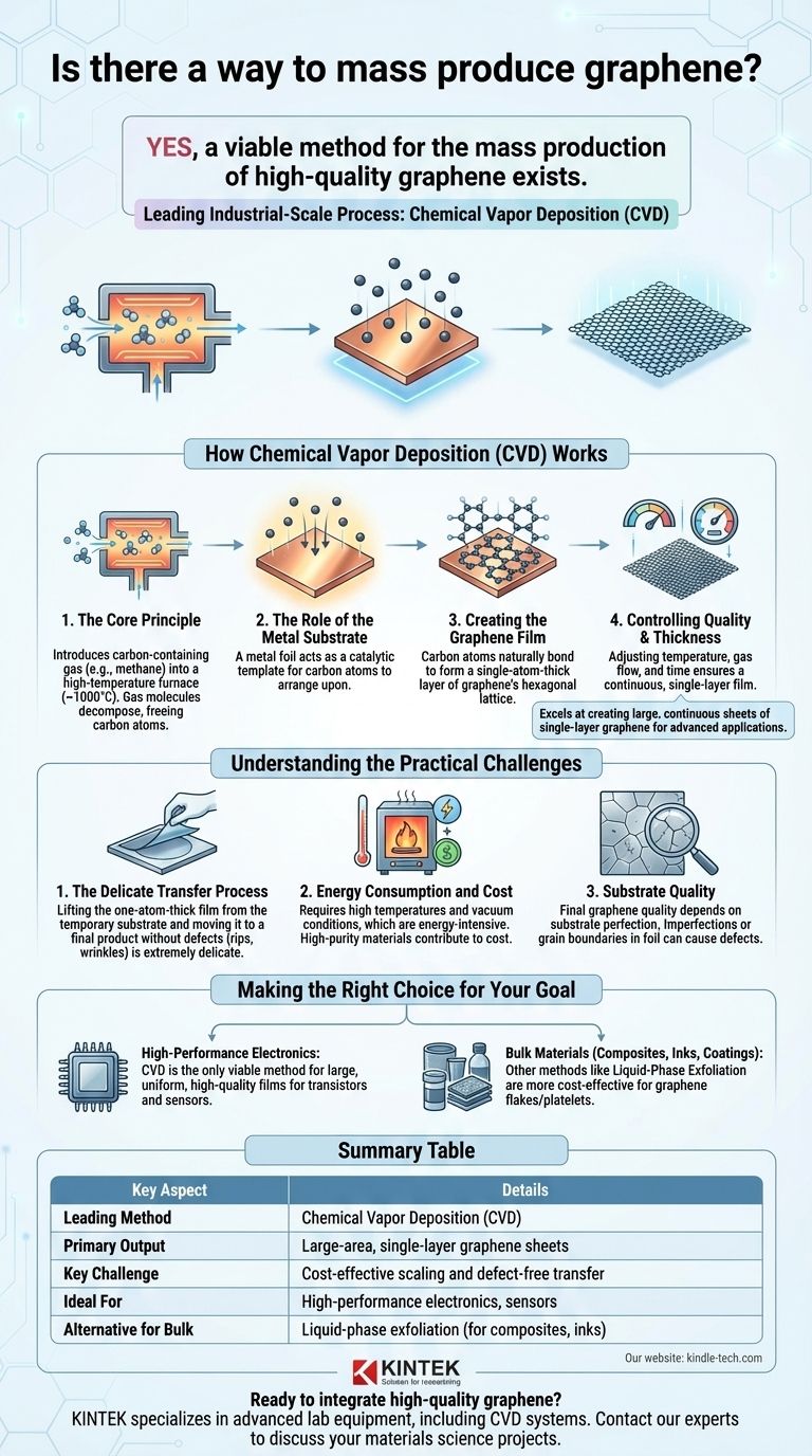
Yes, a viable method for the mass production of high-quality graphene exists. The leading industrial-scale process is known as Chemical Vapor Deposition (CVD), which excels at creating large, continuous sheets of single-layer graphene suitable for advanced electronics and materials science. This method involves growing a one-atom-thick film of carbon on a metal substrate inside a high-temperature furnace.
While the technology to produce large-area graphene is well-established, the term "mass production" is nuanced. The primary challenge has shifted from simply making graphene to scaling the process cost-effectively and perfecting the transfer of the delicate film from its growth substrate to a final product without introducing defects.
How Chemical Vapor Deposition (CVD) Works
The CVD process is a precise, bottom-up approach to building a perfect sheet of graphene atom by atom. It is the gold standard for applications requiring pristine, large-area films.
The Core Principle
The fundamental concept involves introducing a carbon-containing gas, typically methane, into a very hot reaction chamber (~1000°C). At this temperature, the gas molecules decompose, freeing individual carbon atoms to be used as building blocks.
The Role of the Metal Substrate
Inside the furnace, a sheet of a metallic foil, often copper, acts as a catalytic substrate. The hot metal surface helps break down the hydrocarbon gas and provides a perfect template for the carbon atoms to arrange themselves upon.
Creating the Graphene Film
As free carbon atoms land on the hot metal surface, they naturally bond to each other, forming the signature hexagonal lattice structure of graphene. This process continues until a complete, single-atom-thick layer covers the entire surface of the metal substrate.
Controlling Quality and Thickness
The CVD process offers a high degree of control. By carefully adjusting parameters like the furnace temperature, gas flow rate, and exposure duration, engineers can precisely manage the growth, ensuring the final product is a continuous single layer rather than a multi-layer film.
Understanding the Practical Challenges
While CVD successfully produces high-quality graphene, scaling it to an industrial level presents several engineering hurdles that are critical to understand.
The Delicate Transfer Process
Graphene grown via CVD is created on a temporary metal foil. To be useful, this one-atom-thick film must be carefully lifted off the metal and moved to its final substrate, such as a silicon wafer. This transfer step is extremely delicate and a primary source of defects like rips, wrinkles, or contamination that can degrade the material's performance.
Energy Consumption and Cost
The CVD process requires maintaining extremely high temperatures and vacuum conditions, which are energy-intensive. The cost of the high-purity metal substrates and precursor gases also contributes to the overall expense, creating a barrier to truly low-cost mass production.
Substrate Quality
The final quality of the graphene film is directly dependent on the quality of the metal substrate it grows on. Imperfections or grain boundaries in the copper foil can translate into defects in the graphene film, making the procurement and preparation of large, uniform substrates a critical manufacturing step.
Making the Right Choice for Your Goal
The viability of "mass-produced" graphene depends entirely on the requirements of the end application.
- If your primary focus is high-performance electronics: CVD is the only viable production method, as it is uniquely capable of producing the large, uniform, and high-quality films required for transistors and sensors.
- If your primary focus is bulk materials (e.g., composites, inks, or coatings): Other methods, like liquid-phase exfoliation of graphite, are often more cost-effective for producing large quantities of graphene flakes or platelets where perfect, single-layer sheets are not required.
Ultimately, mastering the scaled production and handling of CVD graphene is the key to unlocking its revolutionary potential in commercial applications.
Summary Table:
| Key Aspect | Details |
|---|---|
| Leading Method | Chemical Vapor Deposition (CVD) |
| Primary Output | Large-area, single-layer graphene sheets |
| Key Challenge | Cost-effective scaling and defect-free transfer |
| Ideal For | High-performance electronics, sensors |
| Alternative for Bulk | Liquid-phase exfoliation (for composites, inks) |
Ready to integrate high-quality graphene into your research or production? KINTEK specializes in providing the advanced lab equipment, including CVD systems and consumables, necessary for graphene research and development. Our expertise can help you overcome the challenges of scaling production and achieving consistent quality. Contact our experts today to discuss how we can support your laboratory's innovative materials science projects.
Visual Guide
Related Products
- Laboratory CVD Boron Doped Diamond Materials
- CVD Diamond Wire Drawing Die Blanks for Precision Applications
- CVD Diamond for Thermal Management Applications
- CVD Diamond Dressing Tools for Precision Applications
- Custom CVD Diamond Coating for Lab Applications
People Also Ask
- What are the advantages of BDD electrodes? Maximize Wastewater Treatment Efficiency and Durability
- What materials are CVD deposition? From Semiconductors to Super-Hard Coatings
- What are the applications of CVD diamonds? From Jewelry to High-Tech Tools
- How much cheaper are CVD diamonds? Save 20-30% on a Genuine Diamond
- What is the demand of CVD diamonds? Driven by Ethics, Purity, and Affordability


