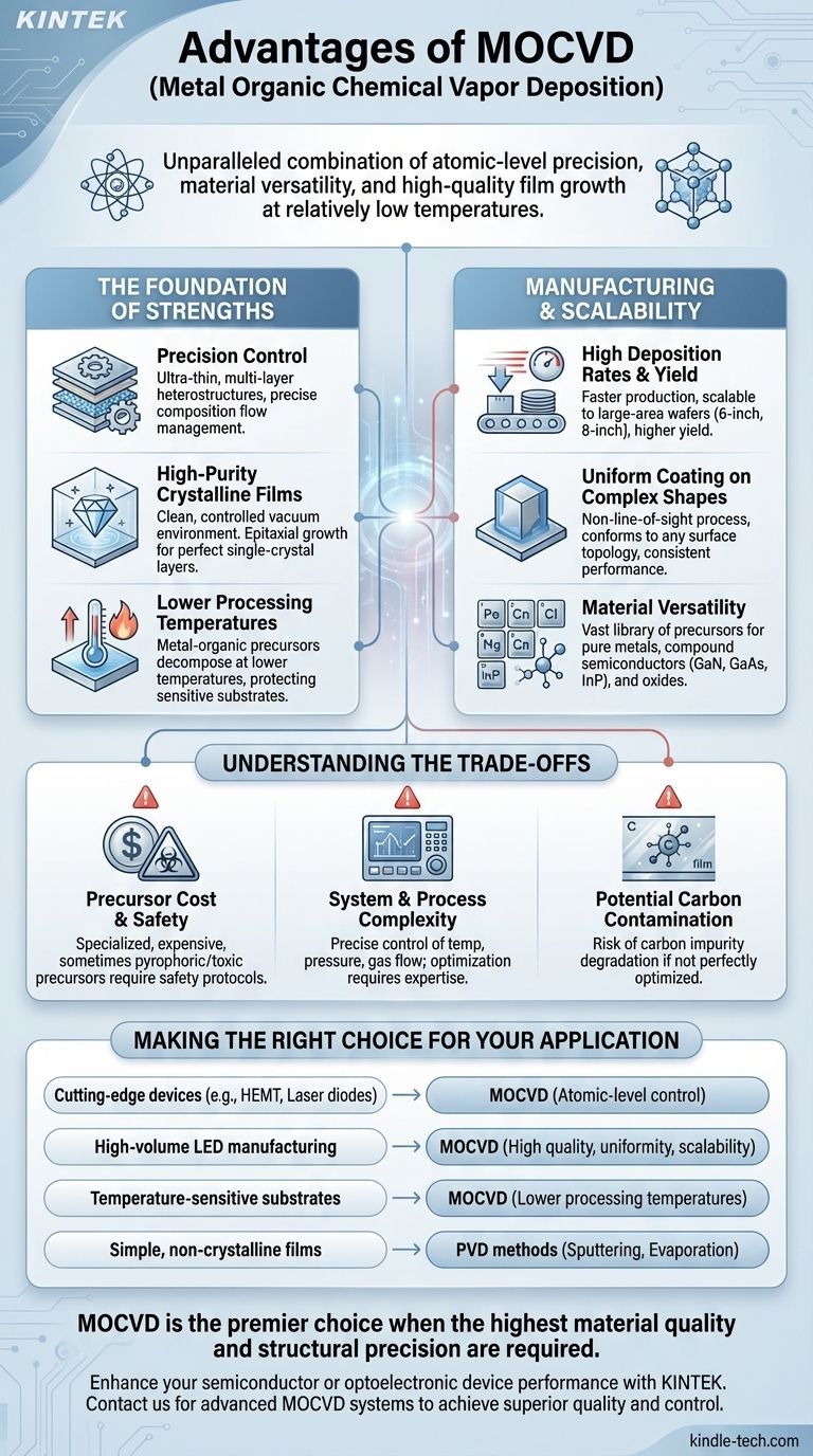
At its core, Metal Organic Chemical Vapor Deposition (MOCVD) offers an unparalleled combination of atomic-level precision, material versatility, and high-quality film growth at relatively low temperatures. This makes it a cornerstone technology for fabricating complex semiconductor devices like high-brightness LEDs, lasers, and high-performance transistors. Its ability to deposit highly pure, uniform crystalline layers over large areas is its defining advantage.
The central advantage of MOCVD lies in its use of metal-organic precursors. These molecules are specifically engineered to decompose at lower temperatures, enabling the growth of high-purity, complex crystal structures on delicate substrates that would be damaged by higher-temperature processes.
The Foundation of MOCVD's Strengths
The unique capabilities of MOCVD stem directly from the chemical nature of its process, which provides a level of control that is difficult to achieve with other methods.
Precision Control Over Composition and Thickness
MOCVD allows for the creation of ultra-thin layers of material, often just a few atomic layers thick. This is critical for modern electronics and optoelectronics.
By precisely managing the flow rates of different precursor gases, engineers can create complex multi-layer structures (heterostructures) with abrupt interfaces and intentionally graded compositions.
High-Purity Crystalline Films
The process is fundamentally clean, taking place in a highly controlled vacuum environment. This results in films with exceptionally high purity, which is essential for achieving desired electronic and optical properties.
MOCVD is particularly adept at epitaxial growth, where the deposited film forms a perfect, single-crystal layer that follows the crystal structure of the underlying substrate.
Lower Processing Temperatures
This is a key differentiator for MOCVD. The metal-organic precursors are designed to react and decompose at lower temperatures compared to the inorganic precursors used in many other CVD techniques.
This lower thermal budget protects the substrate and any previously deposited layers from heat-related damage or diffusion, enabling the fabrication of more complex and sensitive devices.
Manufacturing and Scalability Advantages
Beyond film quality, MOCVD is a robust and scalable process well-suited for high-volume industrial production.
High Deposition Rates and Yield
Compared to some high-precision techniques like Molecular Beam Epitaxy (MBE), MOCVD generally offers higher deposition rates, leading to faster production cycles.
The process is well-understood and can be scaled up to handle large-area wafers (e.g., 6-inch or 8-inch), resulting in a high manufacturing yield and lower cost-per-device.
Uniform Coating on Complex Shapes
As a chemical vapor deposition method, MOCVD is a non-line-of-sight process. The precursor gases flow and conform to any exposed surface within the reactor.
This allows for highly uniform coating of components with complex topographies, ensuring consistent performance across an entire wafer or even on three-dimensional structures.
Versatility Across a Wide Range of Materials
A vast library of metal-organic precursors has been developed for depositing a wide array of materials, including pure metals, compound semiconductors (like GaN, GaAs, InP), and complex oxides. This makes the technique incredibly versatile for R&D and production alike.
Understanding the Trade-offs
While powerful, MOCVD is not without its challenges. An objective assessment requires acknowledging its limitations.
Precursor Cost and Safety
The metal-organic precursors are often highly specialized chemical compounds that can be expensive.
Furthermore, many of these precursors are pyrophoric (ignite spontaneously in air) and toxic, necessitating sophisticated safety protocols and handling systems, which adds to the operational cost.
System and Process Complexity
An MOCVD reactor is a complex piece of equipment requiring precise control over temperature, pressure, and gas flow dynamics. Optimizing a deposition process for a new material or structure can be time-consuming and requires significant expertise.
Potential for Carbon Contamination
The "organic" component of the precursors consists of carbon-hydrogen groups. If the chemical reactions are not perfectly optimized, there is a risk that carbon atoms can be incorporated into the deposited film as an impurity, which can degrade device performance.
Making the Right Choice for Your Application
Selecting MOCVD depends entirely on your specific material, performance, and cost requirements.
- If your primary focus is cutting-edge semiconductor devices (e.g., HEMT, laser diodes): MOCVD's atomic-level control over thickness and composition is a non-negotiable advantage.
- If your primary focus is high-volume LED manufacturing: The combination of high film quality, excellent uniformity, and scalability makes MOCVD the dominant industrial choice.
- If your primary focus is coating temperature-sensitive substrates (e.g., polymers or certain III-V compounds): The lower processing temperatures offered by MOCVD are a critical enabling feature.
- If your primary focus is simple, non-crystalline metallic or oxide films on robust substrates: Simpler, lower-cost PVD methods like sputtering or evaporation may be more economical.
Ultimately, MOCVD is the premier choice when the highest material quality and structural precision are required to achieve superior device performance.
Summary Table:
| Key Advantage | Description |
|---|---|
| Precision Control | Enables atomic-level thickness and composition control for complex heterostructures. |
| High Purity & Epitaxy | Produces ultra-pure, single-crystal films with excellent electronic properties. |
| Low Temperature Processing | Protects sensitive substrates with metal-organic precursors that decompose at lower temperatures. |
| Scalability & Uniformity | Offers high deposition rates and uniform coating on large wafers and complex shapes. |
| Material Versatility | Supports a wide range of materials including III-V semiconductors, oxides, and metals. |
Ready to enhance your semiconductor or optoelectronic device performance with MOCVD technology? KINTEK specializes in providing advanced lab equipment and consumables tailored to your research and production needs. Our expertise in MOCVD systems can help you achieve superior film quality, precise control, and scalable manufacturing. Contact us today to discuss how our solutions can accelerate your innovation and improve your yield.
Visual Guide
Related Products
- Multi Heating Zones CVD Tube Furnace Machine Chemical Vapor Deposition Chamber System Equipment
- 915MHz MPCVD Diamond Machine Microwave Plasma Chemical Vapor Deposition System Reactor
- Microwave Plasma Chemical Vapor Deposition MPCVD Machine System Reactor for Lab and Diamond Growth
- Cylindrical Resonator MPCVD Machine System Reactor for Microwave Plasma Chemical Vapor Deposition and Lab Diamond Growth
- Molybdenum Vacuum Heat Treat Furnace
People Also Ask
- What are the advantages of a multi-zone tube furnace for Sb2S3? Unlock Superior Semiconductor Thin Film Purity
- What is a CVD furnace? The Ultimate Guide to Precision Thin-Film Coating
- What is a CVD tube furnace? A Complete Guide to Thin-Film Deposition
- What is the difference between hot wall CVD and cold wall CVD? Choose the Right System for Your Process
- What is the function of a tube furnace in CVD SiC synthesis? Achieving Ultra-Pure Silicon Carbide Powders