At its core, thin-film technology is about achieving more with less. By depositing material layers that can be just a few atoms thick, we can engineer unique properties, drastically reduce material consumption, and enable the miniaturization of complex devices. This capability is the driving force behind breakthroughs in everything from semiconductors and solar cells to advanced optical coatings and medical implants.
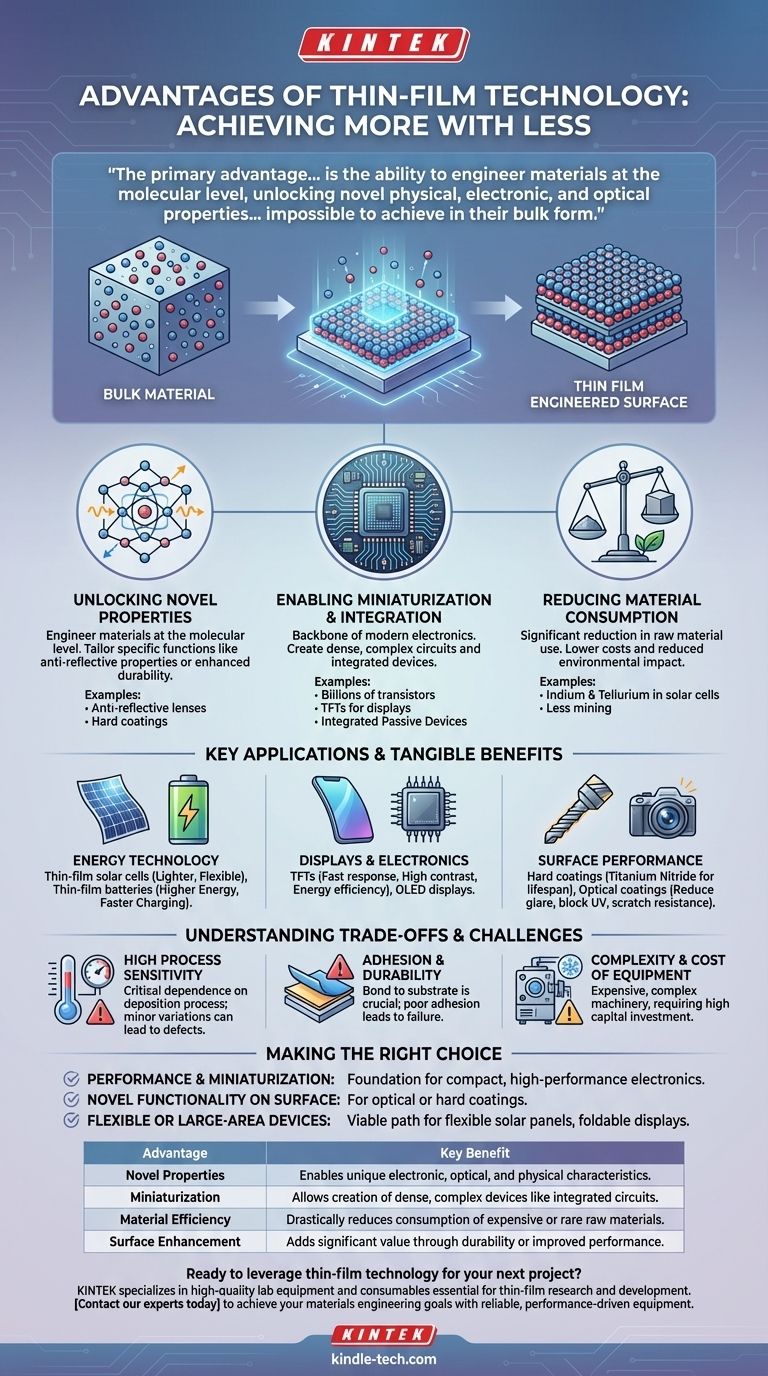
The primary advantage of thin-film technology is not simply making things smaller or using less material. It is the ability to engineer materials at the molecular level, unlocking novel physical, electronic, and optical properties that are impossible to achieve in their bulk form.
The Fundamental Shift: From Bulk Material to Engineered Surfaces
Traditional manufacturing works with "bulk" materials—solid blocks, sheets, or components. Thin-film technology represents a fundamental shift in this paradigm, focusing instead on building devices layer by atomic layer.
Unlocking Novel Properties
When a material's thickness is reduced to the nanometer scale, its properties can change dramatically. The physics governing electrons and light in a constrained, two-dimensional plane is different from that in a three-dimensional bulk material.
This allows engineers to create materials with specific, tailored functions. For example, a simple optical lens can be transformed with an anti-reflective thin film, or a standard cutting tool can be made exceptionally durable with a hard coating.
Enabling Miniaturization and Integration
Thin films are the backbone of modern electronics. They allow for the creation of incredibly dense and complex integrated circuits, where billions of transistors are patterned onto a single chip.
This principle extends beyond CPUs. Technologies like thin-film transistors (TFTs) are essential for modern high-resolution displays, and integrated passive devices (IPDs) use thin films to combine resistors, capacitors, and inductors into a single, compact component.
Reducing Material Consumption
The most obvious benefit is the significant reduction in the amount of raw material required. This is especially critical when using expensive or rare materials, such as the indium and tellurium used in some solar cells.
This efficiency lowers manufacturing costs and reduces the environmental impact associated with mining and processing raw materials.
Key Applications and Their Benefits
The theoretical advantages of thin films translate into tangible, real-world performance gains across multiple industries.
Revolutionizing Energy Technology
Thin-film solar cells are a prime example. They are significantly lighter and more flexible than traditional silicon wafers, enabling applications like photovoltaic glazing on buildings or portable, rollable solar chargers.
Likewise, thin-film batteries offer higher energy density, faster charging rates, and a longer lifespan. This improves the performance and form factor of devices ranging from medical implants and smart cards to large-scale green energy storage banks.
Advancing Displays and Electronics
Nearly every modern screen relies on thin-film technology. Thin-film transistors (TFTs) act as microscopic switches controlling each pixel in an LCD or OLED display.
This technology is what gives modern displays their fast response times, high contrast ratios, and improved energy efficiency compared to older screen technologies.
Enhancing Surface Performance
Thin films provide a powerful way to add value to an existing product. Hard coatings, such as titanium nitride, can be applied to machine tools to dramatically increase their lifespan and cutting performance.
Similarly, optical coatings on glasses or camera lenses can reduce glare, block UV light, and resist scratches—all with a layer of material that is invisibly thin.
Understanding the Trade-offs and Challenges
While powerful, thin-film technology is not a universal solution. Its implementation requires navigating specific engineering challenges.
High Process Sensitivity
The properties of a thin film are critically dependent on the deposition process used to create it (e.g., sputtering, chemical vapor deposition). Minor variations in temperature, pressure, or gas composition can lead to defects that ruin the device's performance.
Achieving uniformity and repeatability, especially over large areas, is a significant manufacturing hurdle.
Adhesion and Durability
A film is only as good as its bond to the substrate beneath it. Poor adhesion can cause the film to peel, flake, or delaminate, leading to device failure.
Furthermore, because the layers are so thin, they can be susceptible to mechanical scratches or chemical damage if not protected or designed for a specific operational environment.
Complexity and Cost of Equipment
The machinery required to deposit high-quality thin films is complex and expensive. These systems often require cleanroom environments and high-vacuum conditions, representing a substantial capital investment.
This initial cost can be a barrier to entry for certain applications or smaller-scale production runs.
Making the Right Choice for Your Goal
Deciding to use thin-film technology depends entirely on your primary objective.
- If your primary focus is performance and miniaturization: Thin films are the non-negotiable foundation for creating compact, high-performance electronics like advanced semiconductors and integrated passive devices.
- If your primary focus is novel functionality on a surface: Use thin films for applications like optical coatings or hard coatings, where a microscopic layer provides a macroscopic improvement in performance.
- If your primary focus is creating flexible or large-area devices: Thin-film deposition is the most viable path for manufacturing products like flexible solar panels, foldable displays, or smart windows.
Ultimately, leveraging thin-film technology is about precisely controlling matter at a microscopic scale to solve macroscopic engineering challenges.
Summary Table:
| Advantage | Key Benefit |
|---|---|
| Novel Properties | Enables unique electronic, optical, and physical characteristics not possible with bulk materials. |
| Miniaturization | Allows for the creation of dense, complex devices like integrated circuits and high-resolution displays. |
| Material Efficiency | Drastically reduces consumption of expensive or rare raw materials, lowering costs and environmental impact. |
| Surface Enhancement | Adds significant value through hard coatings for durability or optical coatings for improved performance. |
Ready to leverage thin-film technology for your next project?
KINTEK specializes in providing high-quality lab equipment and consumables essential for thin-film research and development. Whether you are working on next-generation semiconductors, advanced solar cells, or durable surface coatings, our solutions support the precise deposition processes required for success.
Contact our experts today to discuss how we can help you achieve your materials engineering goals with reliable, performance-driven equipment.
Visual Guide
Related Products
- Vacuum Hot Press Furnace Machine for Lamination and Heating
- Electron Beam Evaporation Coating Oxygen-Free Copper Crucible and Evaporation Boat
- Molybdenum Tungsten Tantalum Evaporation Boat for High Temperature Applications
- Lab Blown Film Extrusion Three Layer Co-Extrusion Film Blowing Machine
- Aluminum-Plastic Flexible Packaging Film for Lithium Battery Packaging
People Also Ask
- What role does the high vacuum environment play in sintering graphite film/aluminum composites? Optimize Your Bonding
- What advantages does a vacuum hot press furnace provide for LSLBO ceramic electrolytes? Achieve 94% Relative Density
- Why is it necessary to maintain a high-vacuum environment within a vacuum hot press furnace? Optimize Cu-SiC Sintering
- What is the application value of a vacuum hot press furnace? Unlock High-Density Complex Carbide Ceramics
- How does the vacuum system within a vacuum hot press furnace contribute to the quality of aluminum matrix composites?


