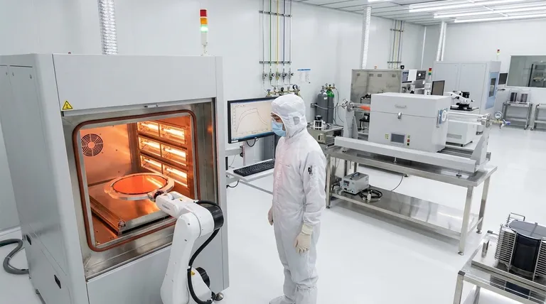
In semiconductor fabrication, annealing is a critical thermal process used to repair crystal lattice damage and electrically activate dopants after ion implantation. The primary types of annealing are Furnace Annealing, Rapid Thermal Annealing (RTA), Flash Lamp Annealing (FLA), and Laser Annealing. Each method offers a different balance between temperature, time, and process control.
While all annealing methods aim to repair crystal damage, the evolution from slow furnaces to ultra-fast lasers is driven by one critical challenge: heating the silicon hot enough to activate dopants without giving them time to diffuse and ruin the nanoscale architecture of modern transistors.
The Core Problem: Repairing Damage Without Diffusion
To understand the different annealing types, you must first grasp the fundamental problem they are designed to solve. The process is a delicate balancing act.
Why Annealing is Necessary
Ion implantation is the standard method for introducing dopant atoms (like boron or phosphorus) into a silicon wafer. This high-energy process is akin to a shotgun blast at the atomic level—it damages the perfect silicon crystal lattice, rendering the implanted region amorphous.
For a transistor to work, two things must happen:
- Lattice Repair: The crystal structure must be repaired.
- Dopant Activation: The dopant atoms must move into the correct positions within the repaired lattice (substitutional sites) to become electrically active.
Both of these require significant thermal energy, which is what annealing provides.
The Diffusion Dilemma
The problem is that heat also causes atoms to move, a process called diffusion. While some movement is needed for activation, too much causes the carefully placed dopants to spread out.
This unwanted diffusion blurs the sharp, well-defined boundaries of the source, drain, and channel regions. In modern transistors with features measured in nanometers, even a tiny amount of diffusion can cause short circuits or device failure. This constant battle between activation and diffusion is the central theme of annealing technology.
A Spectrum of Annealing Techniques
The various annealing methods are best understood as a spectrum of time and temperature control, each developed to better manage the diffusion dilemma for progressively smaller devices.
Furnace Annealing (The Original Method)
This is the classic approach. Wafers are loaded in batches into a horizontal or vertical quartz tube furnace and heated for an extended period, typically from 30 minutes to several hours.
Because of the long duration, temperatures must be kept relatively low (e.g., 600–1000°C) to limit diffusion. This method is simple and processes many wafers at once, making it cost-effective, but its large "thermal budget" (time x temperature) makes it unsuitable for forming the ultra-shallow junctions in advanced devices.
Rapid Thermal Annealing (RTA)
RTA became the industry workhorse for advanced semiconductor nodes. Instead of a slow furnace, RTA processes a single wafer at a time using high-intensity tungsten-halogen lamps.
The wafer can be heated to very high temperatures (e.g., 900–1200°C) in a matter of seconds. This short duration provides enough energy to repair damage and activate dopants with significantly less diffusion than furnace annealing. RTA offers a powerful balance of throughput, performance, and control.
Flash Lamp Annealing (FLA)
For leading-edge nodes, even the seconds-long duration of RTA allows too much diffusion. FLA, also known as millisecond annealing (MSA), uses xenon arc lamps to deliver an intense pulse of energy to the wafer surface.
This heats the top few hundred nanometers of silicon to extreme temperatures (>1200°C) for just a few milliseconds. The bulk of the wafer remains cool, acting as a heat sink that quenches the temperature almost instantly. This achieves very high dopant activation with minimal diffusion, enabling the formation of ultra-shallow junctions.
Laser Annealing (The Precision Tool)
Laser annealing offers the ultimate level of temporal and spatial control. A powerful laser (often an excimer laser) scans across the wafer, heating highly localized spots to their melting point for just nanoseconds.
This "melt" process causes the amorphous layer to liquefy and recrystallize perfectly, incorporating dopants with nearly 100% activation and virtually zero diffusion. While highly effective, laser annealing is complex and has lower throughput than other methods, reserving it for the most critical process steps in the most advanced microchips.
Understanding the Trade-offs
Choosing an annealing technique is a matter of engineering trade-offs. No single method is best for every application.
Thermal Budget and Dopant Diffusion
This is the primary consideration. The total thermal budget determines the amount of diffusion.
- Furnace: High thermal budget, significant diffusion.
- RTA: Moderate thermal budget, controlled diffusion.
- Flash/Laser: Extremely low thermal budget, negligible diffusion.
Process Complexity and Cost
Simpler, batch-based processes are cheaper but less precise.
- Furnace: Low cost, high throughput (batch processing).
- RTA: Moderate cost, moderate throughput (single wafer).
- Flash/Laser: High cost, lower throughput (scanning/single wafer), and complex equipment.
Uniformity and Control
Heating a large, thin silicon wafer uniformly in seconds or milliseconds is a major engineering challenge. Non-uniformity can lead to wafer stress, defects, and inconsistent device performance across the wafer. Advanced RTA and FLA systems require sophisticated sensor and control systems to manage this.
Making the Right Choice for Your Goal
Your choice of annealing method depends entirely on the requirements of the device you are fabricating.
- If your primary focus is on non-critical thermal steps or large feature sizes (>1 µm): Furnace annealing provides a cost-effective solution where dopant diffusion is not a major concern.
- If you are fabricating mainstream logic or memory (e.g., 90nm to 14nm nodes): Rapid Thermal Annealing (RTA) is the essential workhorse, balancing high dopant activation with well-controlled diffusion.
- If you are working with leading-edge nodes (<10nm) requiring ultra-shallow junctions: Millisecond (Flash) or nanosecond (Laser) annealing is necessary to achieve maximum activation with negligible diffusion.
Ultimately, understanding the interplay between temperature, time, and diffusion is the key to selecting the annealing technique that successfully enables your device's performance targets.
Summary Table:
| Annealing Method | Typical Duration | Temperature Range | Key Advantage | Ideal For |
|---|---|---|---|---|
| Furnace Annealing | 30 min - several hours | 600–1000°C | Cost-effective batch processing | Large feature sizes (>1 µm), non-critical steps |
| Rapid Thermal Annealing (RTA) | Seconds | 900–1200°C | Balanced activation & diffusion control | Mainstream logic/memory (90nm - 14nm nodes) |
| Flash Lamp Annealing (FLA) | Milliseconds | >1200°C | Minimal diffusion for ultra-shallow junctions | Leading-edge nodes (<10nm) |
| Laser Annealing | Nanoseconds | Melting point | Near-zero diffusion, maximum activation | Most critical steps in advanced microchips |
Optimize Your Semiconductor Fabrication with KINTEK's Advanced Annealing Solutions
Choosing the right annealing technique is critical for achieving optimal device performance and yield. Whether you're working on large-feature devices or pushing the limits of advanced nodes, KINTEK specializes in providing the precise lab equipment and consumables you need to master thermal processing.
We understand the delicate balance between dopant activation and diffusion control. Our expertise can help you:
- Select the ideal annealing method for your specific semiconductor application
- Achieve superior process control and uniformity
- Maximize device performance while minimizing defects
Ready to enhance your annealing process? Contact our experts today to discuss how KINTEK's solutions can address your specific laboratory challenges and drive your semiconductor innovation forward.
Visual Guide

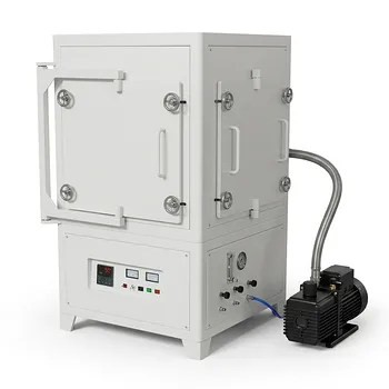
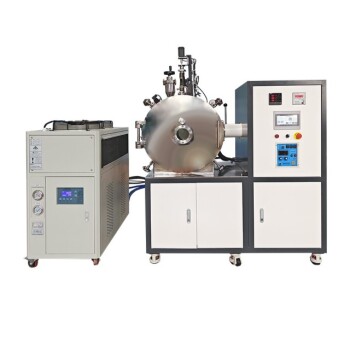
Related Products
- Controlled Nitrogen Inert Hydrogen Atmosphere Furnace
- Vacuum Heat Treat Furnace with Ceramic Fiber Liner
- High Temperature Muffle Oven Furnace for Laboratory Debinding and Pre Sintering
- Mesh belt controlled atmosphere furnace
- Horizontal High Temperature Graphite Vacuum Graphitization Furnace
People Also Ask
- What is the function of an atmosphere control furnace in tungsten carbide production? Achieve High-Purity Synthesis
- Why is a hydrogen atmosphere furnace necessary for W-Cu composite? Unlock Superior Infiltration and Density
- Can hydrogen be used in furnaces? Yes, for Oxide-Free Metal Processing & Rapid Heating
- What is the role of a hydrogen atmosphere furnace in diamond/copper composites? Enhance Your Material Purity
- Why is hydrogen used in furnaces? Achieve Superior Purity and Bright Finishes