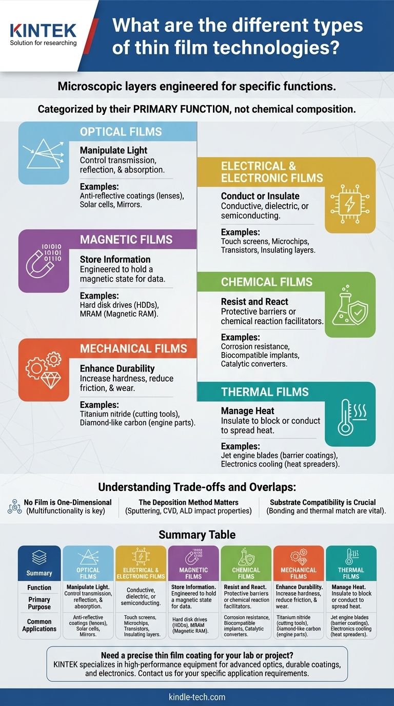
In the world of advanced materials, thin films are microscopic layers engineered to achieve a specific function on a substrate's surface. The primary types are categorized by their dominant property: optical, electrical/electronic, magnetic, chemical, mechanical, and thermal films. Each class is defined not by a single material, but by the physical or chemical behavior it is designed to exhibit.
The key takeaway is that thin film technology is categorized by its primary function, not its chemical composition. Understanding the intended application—whether it's manipulating light, conducting electricity, or resisting wear—is the first step to identifying the correct type of film.
The Functional Categories of Thin Films
A thin film's classification is a direct reflection of the problem it solves. While a single film may have multiple properties, it is typically grouped by its most critical engineered characteristic.
1. Optical Films: Manipulating Light
Optical films are designed to alter the properties of light as it passes through or reflects off a surface. Their primary purpose is to control transmission, reflection, and absorption at specific wavelengths.
Common applications include anti-reflective coatings on eyeglass lenses and camera optics, reflective coatings for mirrors, and specialized coatings on solar cells to maximize light absorption.
2. Electrical & Electronic Films: Conducting and Insulating
This broad category covers films based on their electrical properties. They can be highly conductive, highly insulating (dielectric), or semiconducting.
These films are the bedrock of modern electronics. Examples include the transparent conductive layers in touch screens, the insulating gate oxides in transistors, and the semiconducting layers that form the active parts of microchips.
3. Magnetic Films: Storing Information
Magnetic films are engineered to hold a magnetic state, which allows them to store data. The ability to precisely control the magnetic domains within these microscopic layers is crucial.
The most prominent use for these films has been in data storage, such as the platters inside hard disk drives (HDDs) and in developing technologies like magnetoresistive random-access memory (MRAM).
4. Chemical Films: Resisting and Reacting
Chemical films are designed to interact with their environment. Their purpose is typically to act as a protective barrier or to facilitate a chemical reaction.
This includes films that provide corrosion resistance on metal parts, create biocompatible surfaces on medical implants, or act as catalysts in applications like automotive catalytic converters.
5. Mechanical Films: Enhancing Durability
Mechanical films are applied to a surface to improve its physical properties. The primary goals are to increase hardness, reduce friction (lubricity), and improve resistance to wear and abrasion.
These are often called "hard coatings." Common examples include the titanium nitride coatings that give cutting tools their signature gold color and superior edge retention, and diamond-like carbon (DLC) coatings on engine parts to reduce friction.
6. Thermal Films: Managing Heat
Thermal films are designed to control the flow of heat. They can act either as insulators to block heat or as conductors to spread it away from a critical area.
High-performance applications include thermal barrier coatings that protect jet engine turbine blades from extreme temperatures and heat spreaders used in compact electronics to prevent overheating.
Understanding the Trade-offs and Overlaps
Selecting or designing a thin film is rarely a simple task. The real-world performance of a film depends on a balance of properties and the method used to create it.
No Film is One-Dimensional
A single thin film often must serve multiple functions. For example, the coating on a smartphone screen must be optically transparent (optical), electrically conductive for touch sensing (electrical), and hard enough to resist scratches (mechanical). This multifunctionality is a central challenge in materials engineering.
The Deposition Method Matters
The way a thin film is applied—a process known as deposition—profoundly impacts its final properties. Methods like sputtering, chemical vapor deposition, and atomic layer deposition determine the film's density, purity, internal stress, and uniformity, all of which affect its performance.
Substrate Compatibility is Crucial
A film is only as good as its bond to the underlying material, or substrate. Mismatches in thermal expansion or poor adhesion between the film and the substrate can lead to delamination, cracking, and complete failure of the component.
Selecting the Right Film for Your Application
Your final choice depends entirely on the primary problem you need to solve.
- If your primary focus is durability and wear resistance: You need to investigate mechanical films like diamond-like carbon (DLC) or titanium nitride (TiN).
- If your primary focus is data storage or sensing: Magnetic thin films are the foundational technology for your application.
- If your primary focus is managing light for displays or optics: Optical films, such as anti-reflective or filter coatings, are your starting point.
- If your primary focus is microelectronics: You will be working with a complex stack of electrical, electronic, and insulating films to build functional devices.
- If your primary focus is corrosion protection or biocompatibility: Chemical films designed as barrier layers are the most relevant category.
Understanding these functional categories allows you to select and engineer materials with precision for nearly any technological challenge.
Summary Table:
| Function | Primary Purpose | Common Applications |
|---|---|---|
| Optical | Control light transmission/reflection | Anti-reflective coatings, solar cells, mirrors |
| Electrical/Electronic | Conduct or insulate electricity | Touch screens, microchips, transistors |
| Magnetic | Store data via magnetic state | Hard disk drives (HDDs), MRAM |
| Chemical | Resist corrosion or facilitate reactions | Medical implants, catalytic converters |
| Mechanical | Enhance hardness and reduce wear | Cutting tools (e.g., TiN), engine parts (DLC) |
| Thermal | Manage heat flow (insulate or conduct) | Jet engine blades, electronics cooling |
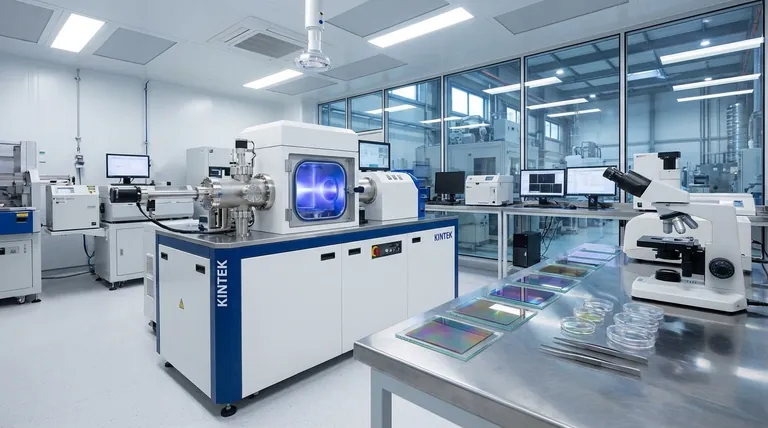
Need a precise thin film coating for your lab or project? KINTEK specializes in high-performance lab equipment and consumables for thin film deposition. Whether you're developing advanced optics, durable mechanical coatings, or next-generation electronics, our solutions ensure the purity, uniformity, and adhesion your research demands. Contact our experts today to discuss how we can support your specific application and material requirements.
Visual Guide
Related Products
- Aluminum-Plastic Flexible Packaging Film for Lithium Battery Packaging
- Thin-Layer Spectral Electrolysis Electrochemical Cell
People Also Ask
- Is there a way to test lithium batteries? Understand Voltage vs. True Health
- What is organic thin film? A Guide to Engineered Molecular Layers for Advanced Tech
- What are the properties of Aluminium (Al) relevant to its use in coatings? High Reflectivity & Conductivity Explored
- What is the thinnest coating? Unlocking Unique Properties at the Atomic Scale
- How to tell if a lithium-ion battery is bad? Spot the critical signs of failure before it's too late.

