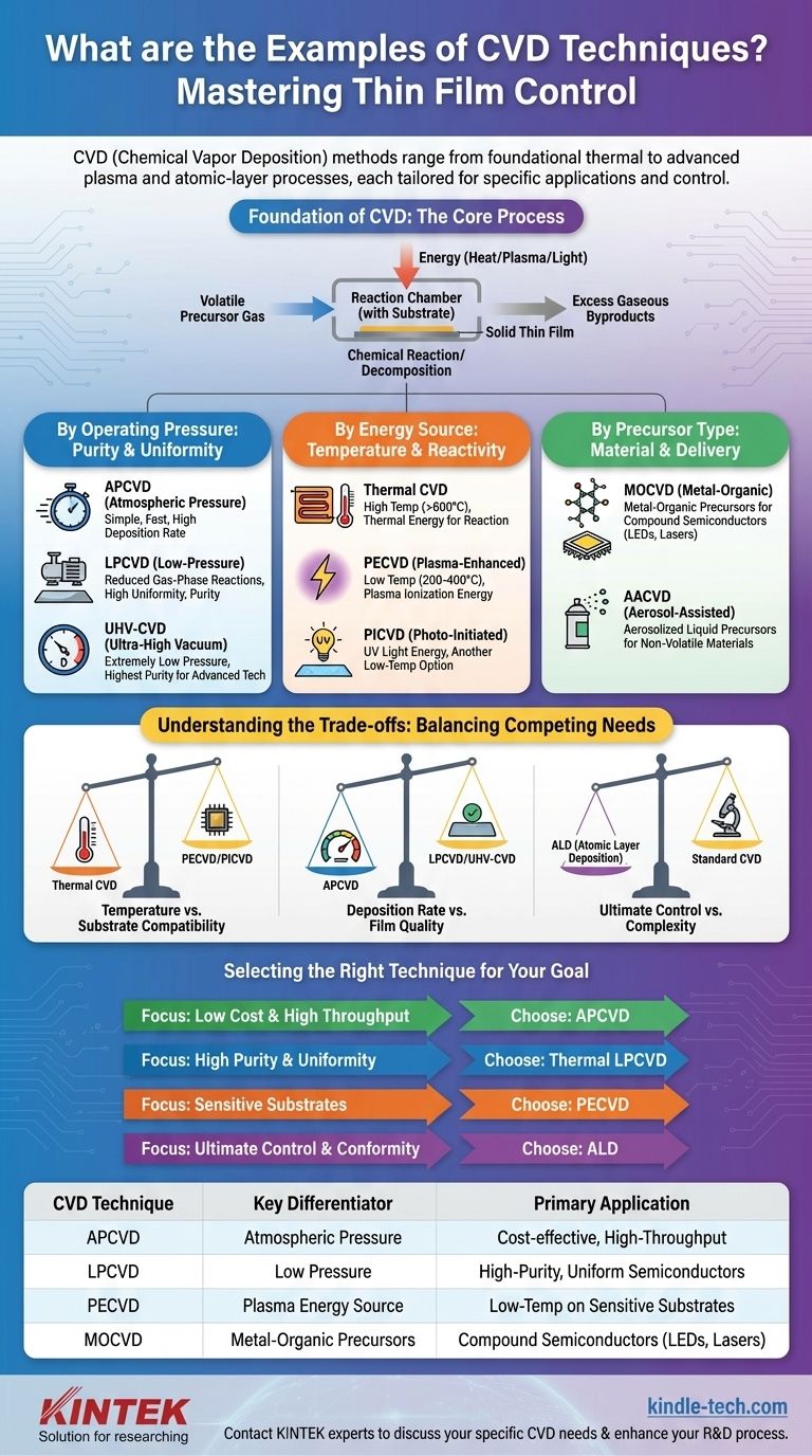
Examples of Chemical Vapor Deposition (CVD) techniques range from foundational thermal methods to highly controlled plasma and atomic-layer processes. The most common variants include Atmospheric Pressure CVD (APCVD), Low-Pressure CVD (LPCVD), Plasma-Enhanced CVD (PECVD), and Metal-Organic CVD (MOCVD). Each variant is tailored to specific applications, materials, and desired film properties.
The variety of CVD techniques exists for one primary reason: control. Each method modifies core process parameters—like pressure, temperature, or the reaction's energy source—to precisely control the growth, composition, and structure of the deposited thin film.
The Foundation of CVD: How it Works
Before exploring the different types, it's essential to understand the core process that unites them. CVD is fundamentally a method for creating a solid material, typically a thin film, from gaseous precursors.
The Core Process: From Gas to Solid
Nearly all CVD techniques follow a few basic steps. First, one or more volatile precursor gases are introduced into a reaction chamber containing the object to be coated, known as the substrate. Second, energy is applied to the chamber, causing the precursor gases to react or decompose on the substrate's surface. Finally, a solid thin film is deposited onto the substrate, and excess gaseous byproducts are removed.
The specific "type" of CVD is defined by how these steps, particularly the energy application and chamber conditions, are managed.
How Different CVD Techniques Are Categorized
The vast number of CVD methods can be understood by grouping them based on the key process parameter they manipulate.
By Operating Pressure
Pressure inside the reaction chamber directly impacts the purity, uniformity, and deposition rate of the film.
- Atmospheric Pressure CVD (APCVD): This process operates at normal atmospheric pressure. It is a relatively simple and fast technique but may result in films with lower purity and conformity compared to other methods.
- Low-Pressure CVD (LPCVD): By reducing the chamber pressure, LPCVD slows down unwanted gas-phase reactions. This leads to highly uniform and pure films, making it a cornerstone of the semiconductor industry.
- Ultra-High Vacuum CVD (UHV-CVD): Operating at extremely low pressures, this technique minimizes contaminants to achieve the highest possible film purity, which is critical for advanced electronics and research.
By Energy Source
The method used to supply energy for the chemical reaction is a major differentiator, especially concerning the required temperature.
- Thermal CVD: This is the conventional method where the substrate is heated to high temperatures (often >600°C). The heat provides the thermal energy needed to initiate the precursor decomposition and surface reaction.
- Plasma-Enhanced CVD (PECVD): This technique uses an electric field to generate a plasma (an ionized gas). The high-energy electrons in the plasma provide the energy for the reaction, allowing deposition to occur at much lower temperatures (200-400°C).
- Photo-Initiated CVD (PICVD): Instead of heat or plasma, this method uses light, typically ultraviolet (UV) radiation, to break down the precursor gases and drive the deposition process. It is another valuable low-temperature technique.
By Precursor Type and Delivery
The chemical nature of the precursor gas defines the material being deposited and requires specialized techniques.
- Metal-Organic CVD (MOCVD): This important subclass uses metal-organic compounds as precursors. MOCVD is essential for creating high-quality compound semiconductor films used in LEDs, lasers, and high-performance transistors.
- Aerosol-Assisted CVD (AACVD): This method is used when precursors are not volatile enough to be easily turned into a gas. The precursor is dissolved in a solvent, an aerosol is generated, and the tiny droplets are transported into the chamber.
Understanding the Trade-offs
Choosing a CVD technique is a matter of balancing competing requirements. There is no single "best" method; the optimal choice depends entirely on the goal.
Temperature vs. Substrate Compatibility
This is the most critical trade-off. Thermal CVD produces excellent films but its high temperatures can damage or destroy sensitive substrates like plastics, polymers, or certain electronic components. PECVD and PICVD solve this problem by enabling high-quality deposition at low temperatures.
Deposition Rate vs. Film Quality
Faster is not always better. Methods like APCVD can offer high deposition rates and throughput, making them cost-effective for simple coatings. However, slower, more controlled processes like LPCVD and UHV-CVD are necessary to achieve the low defect density and high uniformity required for microelectronics.
Ultimate Control vs. Complexity
For the most demanding applications, advanced variants offer unparalleled precision. Atomic Layer Deposition (ALD), a subtype of CVD, uses sequential, self-limiting reactions to deposit a film one single atomic layer at a time. This provides perfect conformity and thickness control but is a very slow and complex process.
Selecting the Right Technique for Your Goal
Your application's primary requirement will dictate the most appropriate CVD technique.
- If your primary focus is low cost and high throughput: APCVD is often the most economical solution for applications where perfect uniformity is not critical.
- If your primary focus is high purity and uniformity for robust materials: Thermal LPCVD is a workhorse of the semiconductor industry for producing exceptional quality films.
- If your primary focus is depositing on temperature-sensitive materials: PECVD is the standard choice, allowing quality film growth on plastics, polymers, and other substrates that cannot withstand high heat.
- If your primary focus is ultimate thickness control and conformity on 3D structures: Atomic Layer Deposition (ALD) is the definitive technique for achieving perfectly uniform, pinhole-free coatings.
Ultimately, choosing the right CVD technique is about matching the method's specific controls to the desired properties of your final thin film.
Summary Table:
| CVD Technique | Key Differentiator | Primary Application |
|---|---|---|
| APCVD | Atmospheric pressure | Cost-effective, high-throughput coatings |
| LPCVD | Low pressure | High-purity, uniform films for semiconductors |
| PECVD | Plasma energy source | Low-temperature deposition on sensitive substrates |
| MOCVD | Metal-organic precursors | Compound semiconductors for LEDs and lasers |
Ready to select the perfect CVD technique for your thin-film application? The experts at KINTEK can help you navigate the trade-offs between temperature, purity, and deposition rate to achieve your specific film properties. Whether you're working with robust semiconductors or temperature-sensitive polymers, KINTEK specializes in providing the right lab equipment and consumables for your laboratory's unique needs. Contact our team today to discuss your project and discover how we can enhance your research and development process!
Visual Guide
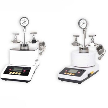
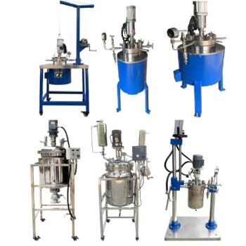
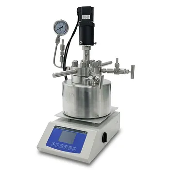
Related Products
- Cylindrical Resonator MPCVD Machine System Reactor for Microwave Plasma Chemical Vapor Deposition and Lab Diamond Growth
- Customer Made Versatile CVD Tube Furnace Chemical Vapor Deposition Chamber System Equipment
- Microwave Plasma Chemical Vapor Deposition MPCVD Machine System Reactor for Lab and Diamond Growth
- Split Chamber CVD Tube Furnace with Vacuum Station Chemical Vapor Deposition System Equipment Machine
- Multi Heating Zones CVD Tube Furnace Machine Chemical Vapor Deposition Chamber System Equipment
People Also Ask
- How are CVD diamonds created? Discover the Science of Lab-Grown Diamond Precision
- What are the advantages of a Microwave Plasma CVD reactor for MCD/NCD coatings? Precision Multilayer Diamond Engineering
- What is the difference between MPCVD and HFCVD? Choose the Right CVD Method for Your Application
- What is MPCVD? Unlock Atom-by-Atom Precision for High-Purity Materials
- Why is argon-rich gas phase chemistry used for UNCD growth? Unlock Precision Nano-Diamond Synthesis