The functions of synthetic graphene are a direct result of its unique physical properties. Because it is a single layer of carbon atoms that is flexible, transparent, and exceptionally conductive of both heat and electricity, its applications span next-generation electronics, energy storage, sensors, and reinforced composite materials. The specific function it can perform is ultimately determined by the quality achieved during its synthesis.
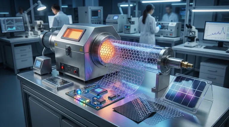
The true value of synthetic graphene lies not just in its remarkable inherent properties, but in our ability to produce it at the right scale and quality for a specific job. The synthesis method, such as Chemical Vapor Deposition (CVD), is what transforms graphene from a laboratory curiosity into a functional engineering material.
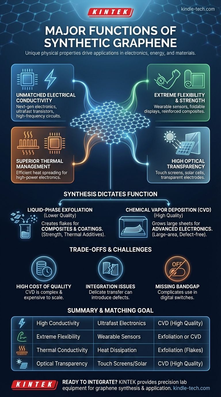
The Foundational Properties Driving Graphene's Functions
Graphene's potential is not based on a single trait, but on the powerful combination of several extreme properties. Understanding these fundamentals is key to seeing why it is being developed for so many different applications.
Unmatched Electrical Conductivity
Graphene has an exceptionally high electrical conductivity. This property makes it a prime candidate for next-generation electronics.
Potential functions include ultrafast transistors, transparent conductive films for touch screens and solar cells, and high-frequency circuits.
Extreme Flexibility and Mechanical Strength
As a single atomic layer, graphene is incredibly flexible and, for its weight, stronger than steel.
This combination is ideal for developing flexible displays, wearable electronic sensors, and foldable batteries. It can also be added to polymers to create ultra-strong, lightweight composite materials.
Superior Thermal Management
Graphene is one of the most thermally conductive materials ever discovered. It can efficiently spread and dissipate heat.
This makes it highly valuable for thermal management in electronics, acting as a heat spreader to cool down processors and other high-power components.
High Optical Transparency
Graphene absorbs only a very small fraction of visible light, making it almost completely transparent.
When combined with its electrical conductivity, this property is crucial for applications like transparent electrodes in LEDs, touch panels, and photovoltaic cells, where light must pass through to the active layers.
Why "Synthetic" Graphene is Key to Application
The method used to create graphene is the most critical factor in determining its ultimate function. While naturally occurring graphite is abundant, isolating a single high-quality layer requires precise engineering.
The Challenge of Scale and Quality
The earliest method, mechanical exfoliation, produced pristine graphene flakes perfect for research but far too small for commercial products.
Other methods, like liquid-phase exfoliation, can produce large quantities of graphene flakes but often at a lower electrical quality, making them suitable for composites but not advanced electronics.
The Rise of Chemical Vapor Deposition (CVD)
As noted in research, Chemical Vapor Deposition (CVD) is the most promising technique for creating high-quality graphene over large areas.
CVD involves "growing" a continuous, single-atom-thick sheet of graphene on a substrate. This method is what makes applications like large-panel displays and integrated circuits feasible.
How Synthesis Dictates Function
The perfection of the hexagonal lattice structure is paramount. A large sheet of high-quality CVD graphene enables sophisticated electronics.
In contrast, a slurry of lower-quality graphene flakes from a different synthesis process might be perfect for mixing into plastics to add strength or thermal conductivity. The function is entirely dependent on the form and quality of the synthetic material.
Understanding the Trade-offs and Limitations
Despite its immense potential, deploying synthetic graphene in commercial products faces significant hurdles. Acknowledging these challenges provides a realistic perspective.
The High Cost of Quality
Producing large-area, defect-free graphene via methods like CVD remains a complex and expensive process. This cost is a major barrier to its widespread adoption in consumer electronics and other mass-market goods.
Integration and Transfer Challenges
Graphene produced by CVD must be transferred from its growth substrate to the final device. This transfer process is delicate and can easily introduce wrinkles, tears, and contaminants that degrade the material's performance.
The Missing Bandgap
For some digital electronics, a material needs to be able to stop the flow of electrons completely—to switch "off." Pristine graphene does not have this "bandgap," which complicates its use in certain types of transistors, though significant research is aimed at engineering solutions.
Matching the Graphene to Your Goal
The right type of synthetic graphene is entirely dependent on the intended application. There is no single "best" form of the material.
- If your primary focus is high-performance electronics: You require large-area, high-quality graphene, likely produced via CVD, to leverage its exceptional conductivity and transparency.
- If your primary focus is material reinforcement or thermal additives: Less-perfect and less-expensive graphene flakes, produced via liquid-phase exfoliation, can provide significant benefits in composites and coatings.
- If your primary focus is fundamental research: Mechanically exfoliated graphene remains the gold standard for studying the material's pure, intrinsic properties without interference from synthesis-related defects.
Ultimately, understanding the direct link between the synthesis method, material quality, and final properties is the key to unlocking graphene's true potential.
Summary Table:
| Function | Key Property | Primary Application |
|---|---|---|
| Ultrafast Electronics | High Electrical Conductivity | Transistors, Circuits |
| Flexible & Strong Composites | Extreme Flexibility & Strength | Wearable Sensors, Lightweight Materials |
| Efficient Heat Dissipation | Superior Thermal Conductivity | Thermal Management in Electronics |
| Transparent Conductive Layers | High Optical Transparency | Touch Screens, Solar Cells |
Ready to integrate synthetic graphene into your lab's projects? KINTEK specializes in high-quality lab equipment and consumables, including tools for graphene synthesis and application. Whether you're advancing electronics or developing new materials, our expertise ensures you get the right solutions for your research. Contact us today to discuss how we can support your laboratory's innovation with precision equipment tailored to your needs.
Visual Guide
Related Products
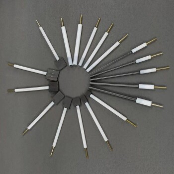
- Carbon Graphite Plate Manufactured by Isostatic Pressing Method
- Graphite Disc Rod and Sheet Electrode Electrochemical Graphite Electrode
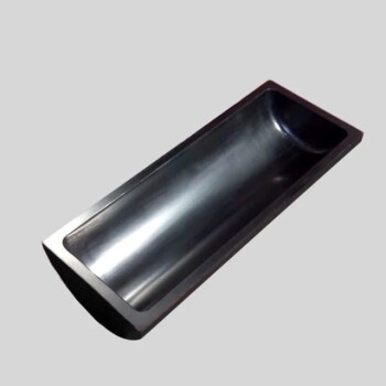
- Carbon Graphite Boat -Laboratory Tube Furnace with Cover
- High Purity Pure Graphite Crucible for Electron Beam Evaporation
- Ultra-High Temperature Graphite Vacuum Graphitization Furnace
People Also Ask
- How is isostatic pressing distinguished from conventional pressing? Unlock Superior Uniformity and Density
- What is the difference between CIP and HIP? A Guide to Choosing the Right Process
- What is isostatic graphite? The Ultimate Material for High-Tech and High-Temperature Applications
- What is the process of isostatic graphite manufacturing? Achieve Unmatched Material Uniformity and Performance
- Why Use an Isostatic or High-Precision Hydraulic Press for Li/LLZO/Li Batteries? Master Solid-State Interfaces