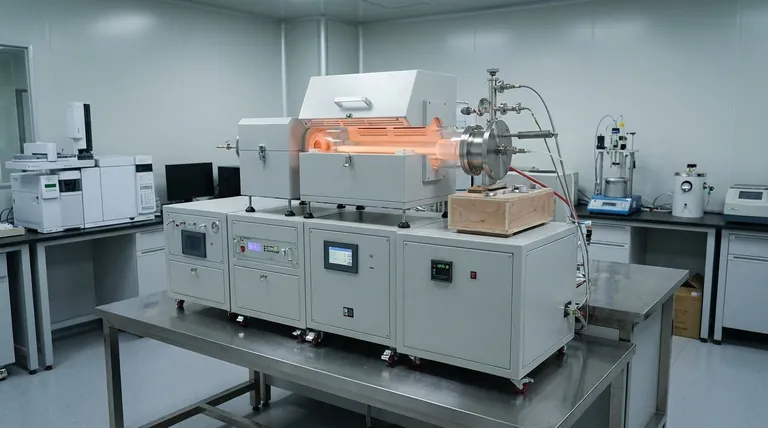
At its core, Chemical Vapor Deposition (CVD) is a family of processes, not a single method. The primary methods are distinguished by the pressure they operate under and how they supply the energy needed to drive the reaction, including thermal, plasma, or light-based techniques. The most common industrial variants include Atmospheric Pressure CVD (APCVD), Low-Pressure CVD (LPCVD), and Plasma-Enhanced CVD (PECVD).
The fundamental difference between CVD methods is the energy source used to initiate the chemical reaction that forms the film. Choosing the right method is a matter of balancing the required deposition temperature, the sensitivity of the substrate material, and the desired quality of the final coating.
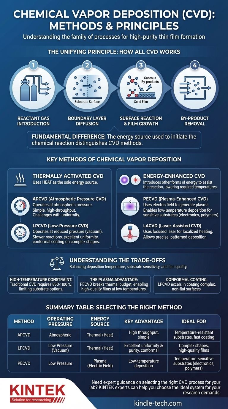
The Unifying Principle: How All CVD Works
Before examining the differences, it's crucial to understand that all CVD methods share a common sequence of events. The goal is to transport chemical precursors in a gas phase to a substrate where they react to form a solid, high-purity thin film.
The Foundational Steps
The process can be broken down into a few key stages.
First, reactant gases are introduced into a reaction chamber. These gases flow towards the substrate, which is the material to be coated.
The Boundary Layer
A thin boundary layer of gas forms over the substrate surface. The reactants must diffuse through this layer to reach the surface.
Surface Reaction and Film Growth
Once on the surface, the precursor molecules are adsorbed. A chemical reaction then occurs, forming the desired solid film and releasing gaseous by-products.
Removal of By-products
These volatile by-products desorb from the surface, diffuse back through the boundary layer, and are then swept out of the chamber, leaving behind a pure, dense film.
Key Methods of Chemical Vapor Deposition
The "best" CVD method depends entirely on the material being deposited and the substrate it's being deposited onto. The primary variations are designed to control the reaction conditions, especially temperature.
Thermally Activated CVD
This is the most traditional category, using heat as the sole energy source to break down the precursor gases.
Atmospheric Pressure CVD (APCVD) operates at standard atmospheric pressure. It is a relatively simple, fast, and high-throughput process but can sometimes struggle with film uniformity and purity.
Low-Pressure CVD (LPCVD) operates at a reduced pressure (vacuum). This slows the gas-phase reactions, allowing precursors to cover complex shapes more evenly and resulting in films with excellent uniformity and higher purity.
Energy-Enhanced CVD
These advanced methods introduce another form of energy to assist the reaction, most often to reduce the high temperatures required by purely thermal methods.
Plasma-Enhanced CVD (PECVD) is one of the most significant variants. It uses an electric field to generate a plasma (an ionized gas), which provides the energy for the chemical reaction. This allows deposition to occur at much lower temperatures.
Laser-Assisted CVD (LACVD) uses a focused laser beam to heat a specific area of the substrate. This allows for precise, patterned deposition without heating the entire object.
Understanding the Trade-offs
The primary limitation of traditional CVD is the extremely high temperature required, often between 850-1100°C. This is the central problem that most alternative CVD methods are designed to solve.
The High-Temperature Constraint
Many important substrate materials, such as polymers or certain semiconductor components, simply cannot withstand the heat of conventional thermal CVD. This severely limits its application.
The Plasma Advantage
PECVD and other energy-assisted methods break this thermal budget constraint. By using plasma to energize the precursors, high-quality, dense films can be grown at temperatures low enough for sensitive electronics and other advanced materials.
Quality and Control
While more complex, advanced CVD methods offer superior control. By adjusting parameters like pressure, gas composition, and plasma power, technicians can fine-tune the film's chemical composition, crystal structure, and grain size. This leads to materials with exceptional hardness, purity, and performance, as seen in the production of high-quality graphene.
Conformal Coating Capability
A key strength of many CVD processes, particularly LPCVD, is their "wrap-around" capability. Because the precursors are in a gas phase, they can coat complex, non-flat surfaces with a highly uniform film, a significant advantage over line-of-sight deposition methods.
Making the Right Choice for Your Goal
Selecting the appropriate CVD technique requires aligning the process capabilities with your primary objective for the thin film.
- If your primary focus is high-throughput coating on a temperature-resistant substrate: APCVD is often the most cost-effective and fastest choice.
- If your primary focus is exceptional film uniformity and purity on complex shapes: LPCVD is the standard for producing high-quality, conformal films when the substrate can handle the heat.
- If your primary focus is depositing high-quality film on a temperature-sensitive substrate: PECVD is the definitive solution, enabling advanced coatings for electronics, polymers, and other delicate components.
Ultimately, mastering Chemical Vapor Deposition is about choosing the right tool to deliver the precise energy needed to build your material, layer by atomic layer.
Summary Table:
| Method | Operating Pressure | Energy Source | Key Advantage | Ideal For |
|---|---|---|---|---|
| APCVD | Atmospheric | Thermal (Heat) | High throughput, simple | Temperature-resistant substrates, fast coating |
| LPCVD | Low Pressure (Vacuum) | Thermal (Heat) | Excellent uniformity & purity, conformal coating | Complex shapes, high-quality films |
| PECVD | Low Pressure | Plasma (Electric Field) | Low-temperature deposition | Temperature-sensitive substrates (electronics, polymers) |
Need expert guidance on selecting the right CVD process for your lab's specific materials and substrates?
KINTEK specializes in providing high-performance lab equipment and consumables for all your deposition needs. Our experts can help you choose the ideal system to achieve the film quality, uniformity, and throughput your research demands.
Contact our team today to discuss your project and discover how KINTEK's solutions can enhance your laboratory's capabilities.
Visual Guide
Related Products
- Chemical Vapor Deposition CVD Equipment System Chamber Slide PECVD Tube Furnace with Liquid Gasifier PECVD Machine
- RF PECVD System Radio Frequency Plasma-Enhanced Chemical Vapor Deposition RF PECVD
- Microwave Plasma Chemical Vapor Deposition MPCVD Machine System Reactor for Lab and Diamond Growth
- Customer Made Versatile CVD Tube Furnace Chemical Vapor Deposition Chamber System Equipment
- 915MHz MPCVD Diamond Machine Microwave Plasma Chemical Vapor Deposition System Reactor
People Also Ask
- What are the core advantages of PE-CVD in OLED encapsulation? Protect Sensitive Layers with Low-Temp Film Deposition
- How expensive is chemical vapor deposition? Understanding the True Cost of High-Performance Coating
- What is plasma enhanced chemical vapor deposition PECVD equipment? A Guide to Low-Temperature Thin Film Deposition
- What types of substrates are used in CVD to facilitate graphene films? Optimize Graphene Growth with the Right Catalyst
- Why is Chemical Vapor Deposition (CVD) equipment uniquely suited for constructing hierarchical superhydrophobic structures?


