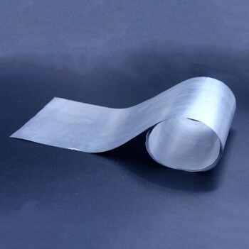
In essence, Aluminum sputtering is a highly controlled physical process used to deposit an ultra-thin, uniform layer of aluminum onto a surface. It involves bombarding a solid aluminum target with energized gas ions inside a vacuum chamber, which physically knocks aluminum atoms off the target. These ejected atoms then travel and condense onto a nearby substrate, such as a silicon wafer or glass, forming a high-quality metallic film.
Sputtering is not a chemical reaction or a melting process. Instead, think of it as a form of "atomic sandblasting," where individual atoms are precisely dislodged and redeposited to build a film one atom at a time, ensuring exceptional purity and adhesion.
How Sputtering Works: A Step-by-Step Breakdown
To understand why sputtering is so widely used, it's helpful to visualize the physical mechanism. The entire process takes place within a sealed, high-vacuum chamber to ensure the purity of the final film.
The Vacuum Chamber Environment
First, the chamber is evacuated to remove air and other contaminants. A pure, inert gas, almost always Argon, is then introduced at a very low pressure.
Generating the Plasma
A strong electric field is applied within the chamber, with the aluminum target acting as the negative electrode (cathode) and the substrate often near the positive electrode (anode). This field energizes the Argon gas, stripping electrons from the atoms and creating a plasma—a glowing, ionized gas.
Bombardment and Ejection
The positively charged Argon ions are accelerated by the electric field and slam into the negatively charged aluminum target. This high-energy collision has enough force to physically knock out, or "sputter," individual aluminum atoms from the target's surface.
Deposition onto the Substrate
These ejected aluminum atoms travel in a straight line through the vacuum chamber until they strike the substrate. Upon impact, they condense and stick to the surface, gradually building up a thin, uniform film with excellent adhesion.
Key Advantages of the Sputtering Process
Sputtering is a dominant technique in many high-tech industries because of its unique combination of precision, control, and material quality.
Superior Adhesion and Coverage
Because the sputtered atoms arrive at the substrate with significant kinetic energy, they embed slightly into the surface. This results in a film with very strong adhesion that is difficult to peel or flake off.
High Purity and Uniformity
The high-vacuum environment prevents unwanted reactions with air, ensuring the deposited aluminum film is exceptionally pure. The process also allows for excellent control over film thickness and uniformity across large surfaces like silicon wafers.
Versatility with Materials
Sputtering is a physical process, not a thermal one. This makes it ideal for depositing materials with very high melting points, like many metals and alloys, which are difficult or impossible to deposit using traditional evaporation methods.
Suitability for Mass Production
The process is highly reproducible and controllable, making it a perfect fit for mass production environments, such as in the manufacturing of semiconductors, hard drives, and optical devices.
Understanding the Trade-offs
While powerful, sputtering is not a universal solution. Understanding its inherent limitations is key to using it effectively.
Requirement for High Vacuum
Sputtering systems require sophisticated and expensive high-vacuum equipment. This makes the initial setup cost higher than some other deposition methods and adds to operational complexity.
Relatively Slow Deposition Rates
Compared to some chemical vapor deposition (CVD) techniques, sputtering can be a slower process. Building up thicker films (multiple micrometers) can be time-consuming.
Line-of-Sight Deposition
Sputtered atoms travel in roughly straight lines from the target to the substrate. This can make it challenging to evenly coat highly complex, three-dimensional shapes with deep trenches or undercuts.
Making the Right Choice for Your Application
Choosing aluminum sputtering depends entirely on your final goal. The process excels where film quality, purity, and adhesion are more important than raw deposition speed or cost.
- If your primary focus is semiconductor manufacturing: Sputtering is the industry standard for creating the fine aluminum interconnects and contact layers on integrated circuits due to its purity and uniformity.
- If your primary focus is creating optical coatings: The process is ideal for depositing the highly reflective aluminum layers found in mirrors, CDs, and other optical components.
- If your primary focus is research and development: Sputtering offers the precise control needed to create novel thin films and test the properties of new alloys that are difficult to produce by other means.
Ultimately, aluminum sputtering is a foundational technology that enables the creation of high-performance materials critical to the modern electronic and optical worlds.
Summary Table:
| Feature | Benefit |
|---|---|
| Physical Vapor Deposition | Ensures high-purity films without chemical reactions. |
| High-Vacuum Environment | Prevents contamination for superior film quality. |
| Excellent Adhesion | Creates durable, long-lasting coatings. |
| Uniform Thickness | Provides consistent results across large surfaces like wafers. |
| Material Versatility | Ideal for metals with high melting points. |
Ready to achieve superior thin film deposition in your lab?
KINTEK specializes in high-performance lab equipment and consumables for precise processes like aluminum sputtering. Whether you are developing next-generation semiconductors, optical coatings, or advanced materials research, our solutions deliver the purity, uniformity, and control you need.
Contact our experts today to discuss how we can support your laboratory's specific requirements with reliable, high-quality equipment.