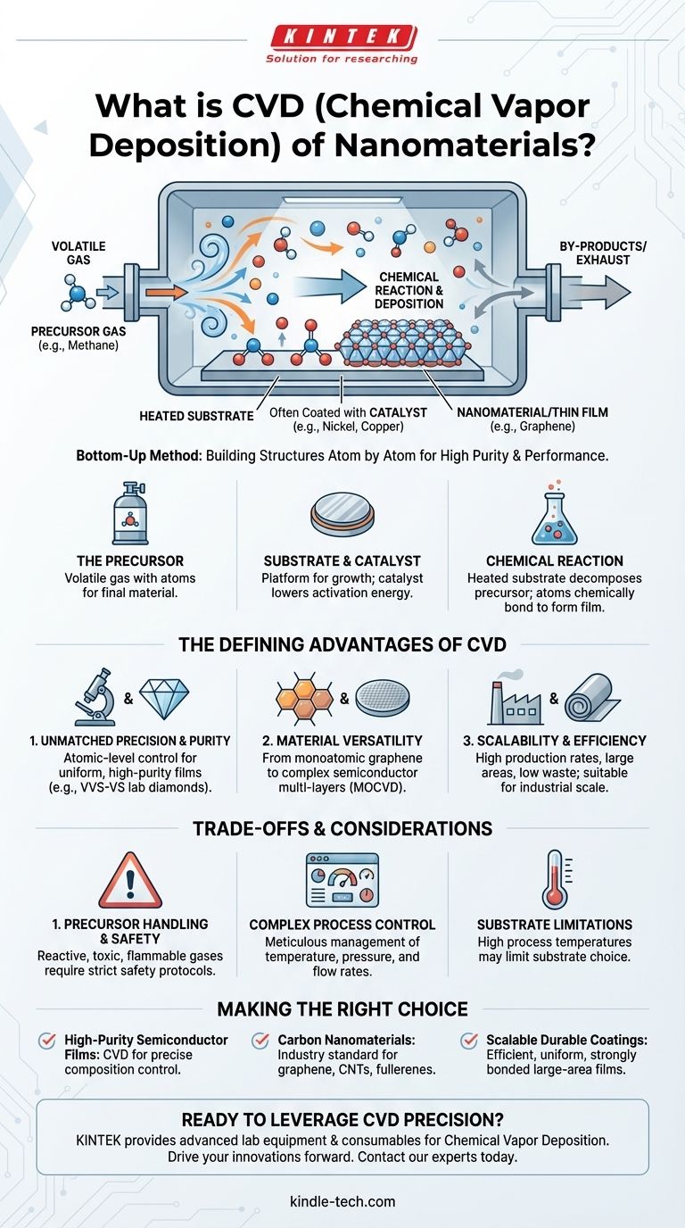
At its core, Chemical Vapor Deposition (CVD) is a "bottom-up" method for creating high-purity, high-performance nanomaterials and thin films. It works by introducing a gas, known as a precursor, into a chamber where it reacts on the surface of a heated object, or substrate. This chemical reaction decomposes the gas and deposits a solid material, building the desired structure atom by atom.
The fundamental advantage of CVD is its use of controlled chemical reactions to build materials. This provides a level of precision over purity, structure, and composition that is critical for advanced applications like semiconductors and carbon nanomaterials.
How CVD Fundamentally Works
To understand the power of CVD, it's essential to grasp its core three components: the precursor, the substrate, and the reaction environment. These elements work in concert to construct materials with atomic precision.
The Gaseous Precursor
The process begins with the precursor, a volatile gas containing the atoms needed for the final material. For example, to create graphene (a carbon nanomaterial), a hydrocarbon gas like methane is often used as the precursor.
The Substrate and Catalyst
The precursor gas is introduced into a reaction chamber containing a substrate, which is the material upon which the new film or nanostructure will be grown. Often, the substrate is coated with a catalyst (like nickel or copper) that lowers the energy needed to activate the chemical reaction.
The Chemical Reaction
This is the key step that separates CVD from purely physical methods. The heated substrate causes the precursor gas to react and decompose. The desired atoms chemically bond to the substrate surface, forming a solid, uniform film. Any unwanted by-products are simply removed from the chamber by the gas flow.
The Defining Advantages of CVD
CVD is a dominant technique in nanotechnology and semiconductor manufacturing because of a distinct set of advantages that are difficult to achieve with other methods.
Unmatched Precision and Purity
Because it builds materials through chemical bonds at the atomic level, CVD offers exceptional control over the final product. This allows for the creation of highly uniform films with excellent purity, thickness, and microstructure. For lab-grown diamonds, this results in high clarity (VVS-VS) without the metallic inclusions found in other methods.
Material Versatility
The CVD process is remarkably versatile. It can be used to fabricate a wide range of materials, from simple monoatomic structures like graphene to complex multi-layer crystalline structures for semiconducting wafers using specialized techniques like MOCVD (Metal-Organic Chemical Vapor Deposition).
Scalability and Efficiency
Compared to many other nanofabrication techniques, CVD is often faster and more efficient. It can be used to deposit materials over large areas and offers high production rates with low waste generation, making it suitable for industrial-scale manufacturing.
Understanding the Trade-offs and Considerations
No technique is without its challenges. While powerful, implementing CVD requires a clear understanding of its operational complexities to ensure successful outcomes.
Precursor Handling and Safety
The precursor gases used in CVD are by nature chemically reactive. Many can be toxic, flammable, or corrosive, requiring strict safety protocols and specialized handling equipment.
Complex Process Control
The high quality of CVD products is a direct result of meticulous process control. Variables like temperature, pressure, gas flow rates, and precursor concentrations must be precisely managed to achieve consistent and repeatable results. Any deviation can impact the final material's properties.
Substrate Limitations
While CVD can be used with many substrates, the process often requires high temperatures to initiate the chemical reaction. This can limit the choice of substrate materials to those that can withstand the thermal conditions without degrading or warping.
Making the Right Choice for Your Goal
Selecting a synthesis method depends entirely on your end goal. CVD is the premier choice when precision and chemical purity are non-negotiable.
- If your primary focus is high-purity semiconductor films: CVD is the superior choice due to its ability to control film composition and microstructure at the atomic level.
- If your primary focus is synthesizing carbon nanomaterials: This method is an industry standard for consistently growing structures like graphene, carbon nanotubes (CNTs), and fullerenes.
- If your primary focus is scalable production of durable coatings: CVD's efficiency and ability to deposit uniform, strongly bonded films over large areas make it ideal for manufacturing.
Ultimately, mastering CVD is about leveraging controlled chemistry to build the future of materials from the atom up.
Summary Table:
| Key Aspect | Description |
|---|---|
| Core Principle | A "bottom-up" method using chemical reactions to deposit solid materials atom by atom from a gaseous precursor. |
| Primary Advantage | Unmatched precision and control over material purity, structure, and composition. |
| Common Applications | Semiconductor wafers, graphene, carbon nanotubes (CNTs), lab-grown diamonds, and durable coatings. |
| Key Considerations | Requires precise control of temperature, pressure, and gas flow; often involves high temperatures and specialized precursor handling. |
Ready to leverage the precision of CVD for your research or production? KINTEK specializes in providing the advanced lab equipment and consumables needed to master Chemical Vapor Deposition. Whether you are developing next-generation semiconductors, synthesizing carbon nanomaterials, or creating high-performance coatings, our expertise can help you achieve consistent, high-quality results. Contact our experts today to discuss how we can support your specific laboratory needs and drive your innovations forward.
Visual Guide
Related Products
- CVD Diamond Dressing Tools for Precision Applications
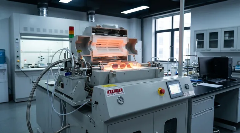
- Multi Heating Zones CVD Tube Furnace Machine Chemical Vapor Deposition Chamber System Equipment
- CVD Diamond Domes for Industrial and Scientific Applications
- CVD Diamond for Thermal Management Applications
- Chemical Vapor Deposition CVD Equipment System Chamber Slide PECVD Tube Furnace with Liquid Gasifier PECVD Machine
People Also Ask
- How do you identify a CVD diamond? The Definitive Guide to Lab-Grown Diamond Verification
- How do CVD diamonds grow? A Step-by-Step Guide to Lab-Grown Diamond Creation
- What are the disadvantages of CVD diamonds? Understanding the trade-offs for your purchase.
- Can CVD diamonds change color? No, their color is permanent and stable.
- Does the chemical vapor deposition be used for diamonds? Yes, for Growing High-Purity Lab Diamonds


