At its core, diode sputtering is a foundational method for creating ultra-thin films of material on a surface. It is a type of physical vapor deposition (PVD) that operates in a vacuum, using a simple two-electrode (diode) system to generate a plasma. This plasma bombards a source material, dislodging atoms that then coat a separate object, known as the substrate.
While the term may sound complex, diode sputtering is simply the most fundamental version of a process that underpins much of modern technology. It works by using high-energy ion bombardment to meticulously transfer atoms from a source to a substrate, offering atomic-level control over the creation of new surfaces.
The Core Mechanism of Sputtering
To truly understand diode sputtering, we must break down the process into its essential stages. Each step occurs within a sealed vacuum chamber to ensure the purity and integrity of the final film.
The Vacuum Environment
First, both the source material (target) and the object to be coated (substrate) are placed in a vacuum chamber. All air is pumped out, creating a near-vacuum.
This vacuum is critical. It prevents atoms from the sputtering target from colliding with air molecules and ensures the resulting film is not contaminated by oxygen, nitrogen, or other atmospheric gases.
Creating the Plasma
An inert gas, most commonly Argon (Ar), is then introduced into the chamber at very low pressure. A strong DC voltage is applied between two electrodes.
The target material is made the cathode (negative electrode), while the substrate holder and chamber walls act as the anode (positive electrode). This simple two-electrode configuration is why the process is called "diode" sputtering. The powerful electric field energizes the free electrons in the chamber, initiating a self-sustaining plasma glow.
The Bombardment Process
The energized electrons collide with the neutral Argon gas atoms, knocking electrons loose from them. This process, called ionization, turns the Argon atoms into positively charged Argon ions (Ar+).
These new, positively charged ions are now aggressively accelerated by the electric field toward the negatively charged target. They strike the target surface with tremendous kinetic energy, physically dislodging, or "sputtering," individual atoms of the target material.
Deposition onto the Substrate
The ejected atoms from the target travel in a straight line through the vacuum. They eventually strike the surface of the substrate, which is strategically placed to intercept this vapor stream.
As these atoms land on the substrate, they condense and bond to its surface, gradually building a thin, uniform film. The process allows for precise control over film thickness, from just a few nanometers to several micrometers.
Understanding the Trade-offs
Diode sputtering is the simplest form of sputtering, but this simplicity comes with significant trade-offs compared to more advanced techniques.
Pro: Simplicity and Cost
The primary advantage of a diode system is its simplicity. The setup is straightforward and relatively inexpensive, making it an excellent tool for research, process development, and demonstrating the fundamental principles of physical vapor deposition.
Con: Low Deposition Rates
Diode sputtering is notoriously slow. The plasma it creates is not very dense, meaning the rate of ion bombardment and subsequent deposition is low. This makes it unsuitable for most high-volume manufacturing where throughput is critical.
Con: Substrate Heating
The process is inefficient. Many of the electrons accelerated from the cathode miss the Argon atoms and instead bombard the substrate, depositing significant heat. This can damage heat-sensitive substrates like plastics or delicate electronic components.
Con: Limited to Conductive Targets
The basic DC diode setup relies on the target being electrically conductive to function as a cathode. To sputter insulating or non-conductive materials (like ceramics), a more complex technique like RF (Radio Frequency) Sputtering is required, which uses an alternating AC field.
Making the Right Choice for Your Goal
While rarely used in modern mass production, understanding diode sputtering is essential for grasping the principles behind the more advanced methods that have replaced it, such as magnetron sputtering.
- If your primary focus is fundamental research or teaching: Diode sputtering is an excellent, low-cost tool for demonstrating the core principles of PVD.
- If your primary focus is high-volume manufacturing: You will almost certainly use a more advanced method like magnetron sputtering, which adds magnets to increase speed and efficiency dramatically.
- If your primary focus is depositing insulating materials: You must use a technique like RF sputtering instead of a DC diode system.
Understanding the principles of diode sputtering provides the essential foundation for mastering all modern thin-film deposition technologies.
Summary Table:
| Aspect | Description |
|---|---|
| Process Type | Physical Vapor Deposition (PVD) |
| Key Components | Cathode (Target), Anode (Substrate), Inert Gas (Argon) |
| Primary Advantage | Simple setup, low cost, excellent for R&D |
| Main Limitation | Low deposition rates, significant substrate heating |
| Best For | Conductive targets, fundamental research, process development |
Ready to Elevate Your Thin-Film Research or Production?
Understanding the fundamentals is the first step. KINTEK specializes in advanced lab equipment and consumables for all your deposition needs. Whether you are moving from basic diode principles to high-throughput magnetron sputtering or require solutions for insulating materials, our expertise can help you achieve precise, high-quality results.
Contact our experts today to discuss how our solutions can optimize your laboratory's efficiency and capabilities.
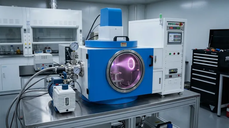
Visual Guide

Related Products
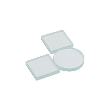
- Laboratory CVD Boron Doped Diamond Materials
- Reference Electrode Calomel Silver Chloride Mercury Sulfate for Laboratory Use
- RF PECVD System Radio Frequency Plasma-Enhanced Chemical Vapor Deposition RF PECVD
- Custom CVD Diamond Coating for Lab Applications
- CVD Diamond for Thermal Management Applications
People Also Ask
- Are CVD diamonds good? Real Diamonds with Ethical Origins & Better Value
- How much cheaper are CVD diamonds? Save 20-30% on a Genuine Diamond
- Are CVD diamonds synthetic? Discover the Truth About Lab-Grown Diamonds
- What materials are CVD deposition? From Semiconductors to Super-Hard Coatings
- What is the purpose of performing anodic polarization on BDD electrodes? Ensure Accurate & Reproducible Research Results