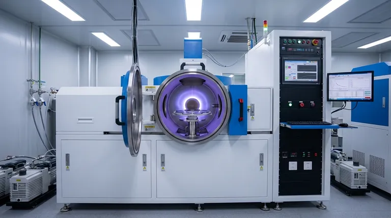
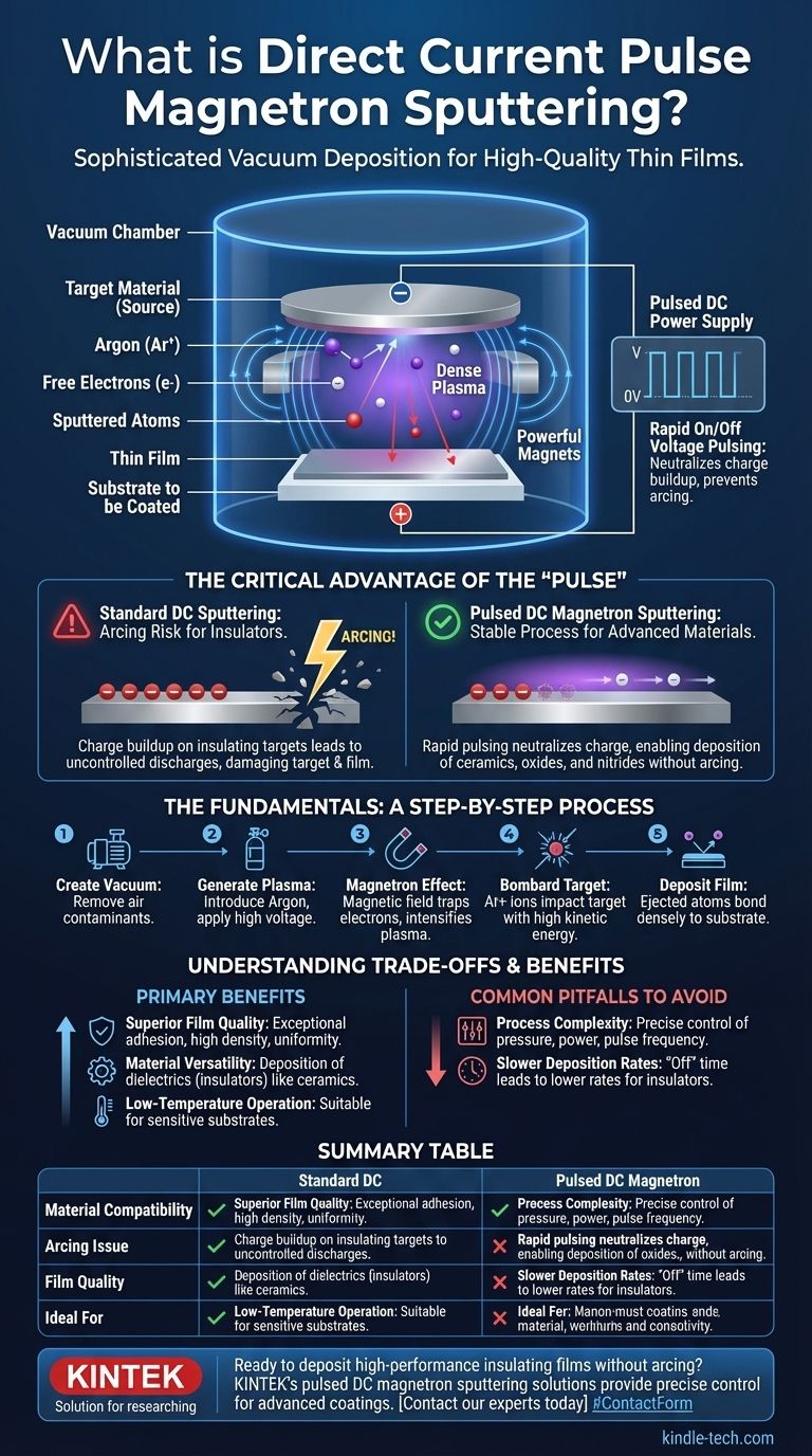
At its core, pulsed direct current (DC) magnetron sputtering is a sophisticated vacuum deposition technique used to create exceptionally high-quality thin films on a substrate. It operates by bombarding a source material (a "target") with ionized gas in a process enhanced by a magnetic field and controlled by a pulsing electrical current, allowing for the precise, atom-by-atom application of a coating. This method is favored for its ability to produce dense, uniform, and highly adherent films from a vast range of materials.
The central challenge with standard DC sputtering is its inability to effectively deposit insulating materials due to electrical charge buildup. Pulsed DC magnetron sputtering solves this by rapidly switching the voltage on and off, which neutralizes this charge, preventing damaging arcs and unlocking the ability to coat substrates with advanced ceramics, oxides, and nitrides.
The Fundamentals: A Step-by-Step Process
Pulsed DC magnetron sputtering, like all sputtering techniques, is a form of Physical Vapor Deposition (PVD). The process unfolds in a highly controlled vacuum environment to ensure the purity of the final film.
Creating the Vacuum Environment
First, the substrate to be coated and the source material (target) are placed inside a sealed vacuum chamber. The chamber is pumped down to a very low pressure, removing ambient air and contaminants that could interfere with the process.
Generating the Plasma
Once the vacuum is established, a small amount of an inert gas, typically Argon, is introduced. A high voltage is applied, which strips electrons from the Argon atoms, creating a plasma—a glowing, ionized gas consisting of positive Argon ions (Ar+) and free electrons.
The Role of the Magnetron
This is where the "magnetron" aspect is critical. Powerful magnets are placed behind the target material. This magnetic field traps the free electrons near the surface of the target, dramatically increasing the probability of them colliding with and ionizing more Argon atoms.
This creates a dense, stable plasma confined directly in front of the target, which significantly increases the efficiency and rate of the sputtering process.
Bombarding the Target
The positive Argon ions in the plasma are accelerated by the electric field and slam into the negatively charged target material with immense kinetic energy. This physical bombardment is forceful enough to knock individual atoms or molecules off the target, ejecting them into the vacuum chamber.
Depositing the Thin Film
These "sputtered" atoms travel through the chamber and land on the substrate, gradually building up a thin, uniform film. Because the sputtered atoms have much higher kinetic energy than particles in other methods like thermal evaporation, they embed more effectively into the substrate, creating a denser and more strongly bonded coating.
The Critical Advantage of the "Pulse"
While the magnetron enhances efficiency, the "pulsed DC" power supply is what makes the technique so versatile. It directly solves a fundamental limitation of continuous DC sputtering.
The Problem with Simple DC: Arcing
When sputtering electrically insulating materials like ceramics or oxides with a standard DC power supply, a positive charge rapidly builds up on the target's surface. This charge buildup can lead to uncontrolled electrostatic discharges known as arcing, which can damage the target, the substrate, and the power supply, while creating defects in the film.
The Solution: Pulsing the Power
A pulsed DC power supply rapidly switches the voltage on and off thousands of times per second. During the brief "off" period, the positive charge on the target is neutralized by electrons from the plasma.
This cycle prevents the charge from ever building up to the point of arcing. This simple but powerful modification stabilizes the process, allowing for the smooth, high-quality deposition of insulating and semi-conductive materials that would otherwise be impossible with standard DC sputtering.
Understanding the Trade-offs and Key Benefits
No single process is perfect for every application. Understanding the advantages of pulsed DC magnetron sputtering helps clarify its ideal uses.
Primary Benefits
- Superior Film Quality: The high energy of sputtered particles results in films with exceptional adhesion, higher density, and greater uniformity.
- Material Versatility: The process works with nearly any material, including metals, alloys, and compounds with very high melting points. The pulsed power supply specifically enables the deposition of dielectrics (insulators) like aluminum oxide and silicon nitride.
- Low-Temperature Operation: Sputtering is a relatively cool process compared to techniques like Chemical Vapor Deposition (CVD), making it suitable for temperature-sensitive substrates like plastics or electronics.
Common Pitfalls to Avoid
- Process Complexity: Achieving optimal results requires precise control over multiple variables, including pressure, power, gas flow, and pulse frequency. It is a more complex setup than simpler methods like thermal evaporation.
- Slower Deposition Rates for Insulators: While pulsing enables the deposition of insulators, the "off" time in the duty cycle can lead to lower deposition rates compared to sputtering conductive metals with continuous DC.
Making the Right Choice for Your Goal
Your specific objective determines whether this technique is the optimal choice.
- If your primary focus is depositing a simple, conductive metal film: Standard DC magnetron sputtering is often sufficient, faster, and more cost-effective.
- If your primary focus is depositing a high-performance ceramic, oxide, or nitride: Pulsed DC magnetron sputtering is the essential and superior technology for achieving a stable, arc-free process and a high-quality insulating film.
- If your primary focus is achieving the absolute best adhesion and film density on a sensitive substrate: The inherent high-energy nature of any magnetron sputtering process makes it a leading candidate.
Ultimately, pulsed DC magnetron sputtering empowers engineers and scientists to apply advanced functional coatings that were once out of reach for conventional PVD methods.
Summary Table:
| Key Feature | Standard DC Sputtering | Pulsed DC Magnetron Sputtering |
|---|---|---|
| Material Compatibility | Primarily conductive metals | Metals, alloys, ceramics, oxides, nitrides |
| Arcing Issue | Common with insulators | Prevented by voltage pulsing |
| Film Quality | Good for metals | Superior density, adhesion, and uniformity |
| Process Complexity | Lower | Higher, requires precise control |
| Ideal For | Simple metal coatings | Advanced functional coatings on sensitive substrates |
Ready to deposit high-performance insulating films without arcing?
Pulsed DC magnetron sputtering from KINTEK is the key to achieving dense, uniform, and highly adherent coatings on even the most sensitive substrates. Our expertise in lab equipment and consumables ensures you get the precise control needed for advanced ceramics, oxides, and nitrides.
Contact our experts today to discuss how our sputtering solutions can elevate your thin film research and production.
Visual Guide
Related Products
- RF PECVD System Radio Frequency Plasma-Enhanced Chemical Vapor Deposition RF PECVD
- Spark Plasma Sintering Furnace SPS Furnace
- Microwave Plasma Chemical Vapor Deposition MPCVD Machine System Reactor for Lab and Diamond Growth
- 915MHz MPCVD Diamond Machine Microwave Plasma Chemical Vapor Deposition System Reactor
- Customer Made Versatile CVD Tube Furnace Chemical Vapor Deposition Chamber System Equipment
People Also Ask
- How does plasma enhance CVD? Unlock Low-Temperature, High-Quality Film Deposition
- What is an example of PECVD? RF-PECVD for High-Quality Thin Film Deposition
- What is plasma enhanced chemical vapour deposition process? Unlock Low-Temperature, High-Quality Thin Films
- What is plasma chemical vapor deposition? A Low-Temperature Thin Film Coating Solution
- What is plasma enhanced chemical vapour deposition PECVD used for? Enable Low-Temp Thin Films for Electronics & Solar


