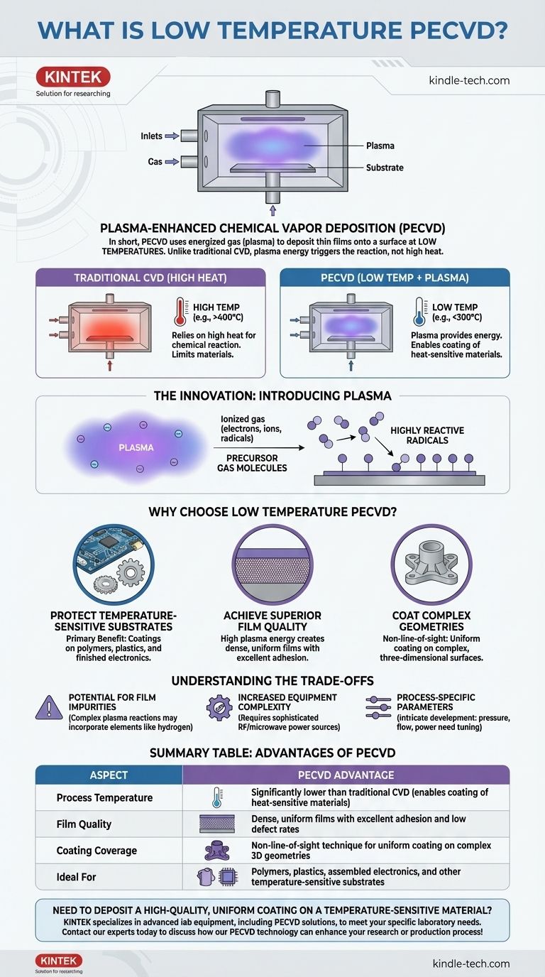
In short, Low Temperature Plasma-Enhanced Chemical Vapor Deposition (PECVD) is a manufacturing process that uses an energized gas, or plasma, to deposit thin films onto a surface. Unlike traditional Chemical Vapor Deposition (CVD), which relies on high heat to trigger chemical reactions, PECVD uses the energy from the plasma to do the work. This critical difference allows for high-quality coatings to be applied at much lower temperatures.
The central takeaway is that PECVD substitutes the high heat of conventional deposition methods with the energy of a plasma. This innovation unlocks the ability to coat temperature-sensitive materials—like plastics, polymers, and complex electronic devices—that would otherwise be damaged or destroyed by high-temperature processes.
Deconstructing the Deposition Process
To understand the value of PECVD, it's essential to first grasp the fundamentals of the technology it enhances.
The Foundation: Chemical Vapor Deposition (CVD)
In a standard CVD process, a substrate (the part to be coated) is placed in a vacuum chamber. Precursor gases containing the desired coating material are then introduced.
High temperatures, often several hundred degrees Celsius, are applied. This heat provides the energy needed to cause a chemical reaction, breaking down the gases and depositing a thin, solid film onto the substrate's surface.
The Innovation: Introducing Plasma
PECVD modifies this process by adding an energy source to create a plasma. A plasma is a state of matter, an ionized gas consisting of free electrons, ions, and reactive neutral species.
This plasma bombards the precursor gas molecules, breaking them apart into highly reactive radicals. These radicals are chemically primed to bond to the substrate surface, even at low temperatures.
The "Low Temperature" Advantage
Because the plasma, not heat, provides the primary energy for the chemical reaction, the entire process can run at significantly lower temperatures.
This allows for the deposition of durable, high-performance films on materials that cannot withstand the thermal stress of conventional CVD, dramatically expanding its range of applications.
Why Choose Low Temperature PECVD?
The decision to use PECVD is driven by a distinct set of advantages that solve specific engineering challenges.
Protecting Temperature-Sensitive Substrates
This is the primary benefit. Materials like polymers, plastics, or fully assembled semiconductor wafers with delicate integrated circuits cannot tolerate the high heat of traditional CVD. PECVD is often the only viable method for applying a high-quality, dense coating to these substrates.
Achieving Superior Film Quality
The high energy of the plasma species helps create very dense and uniform films. This results in coatings with excellent adhesion, low defect rates, and reliable performance, which is critical in fields like optics and electronics.
Coating Complex Geometries
Like all CVD processes, PECVD is not a "line-of-sight" technique. The precursor gases and plasma fill the entire chamber, allowing the reactive species to deposit uniformly on all exposed surfaces. This makes it ideal for coating complex, three-dimensional parts that would be impossible to cover evenly with methods like Physical Vapor Deposition (PVD).
Understanding the Trade-offs
While powerful, PECVD is not a universal solution. Understanding its limitations is key to making an informed decision.
Potential for Film Impurities
The chemical reactions within the plasma can be complex. In some cases, elements from the precursor gases (such as hydrogen) can become incorporated into the final film. For applications demanding the absolute highest material purity, this can be a drawback compared to high-temperature thermal CVD.
Increased Equipment Complexity
Generating and sustaining a stable, uniform plasma requires sophisticated radio-frequency (RF) or microwave power sources and matching networks. This makes PECVD systems more complex and often more expensive than their simpler thermal CVD counterparts.
Process-Specific Parameters
PECVD process development can be more intricate than for thermal CVD. Factors like gas pressure, flow rates, plasma power, and frequency must be precisely tuned to achieve the desired film properties, requiring significant process expertise.
How to Apply This to Your Project
Your choice of deposition technology should be guided by your primary goal and substrate material.
- If your primary focus is coating heat-sensitive substrates: PECVD is the definitive choice, as it uses plasma energy to enable deposition at temperatures that will not damage materials like plastics or finished electronics.
- If your primary focus is achieving the highest possible film purity for a durable substrate: A high-temperature process like Low-Pressure CVD (LPCVD) may be a better option, provided your substrate can tolerate the heat.
- If your primary focus is coating complex 3D shapes at low cost: PECVD provides the conformal coverage of a gas-phase process, but you must weigh its equipment cost against the thermal limitations of your part.
By understanding the fundamental trade-off between thermal energy and plasma energy, you can confidently select the deposition technique that aligns with your material, substrate, and performance requirements.
Summary Table:
| Aspect | PECVD Advantage |
|---|---|
| Process Temperature | Significantly lower than traditional CVD (enables coating of heat-sensitive materials) |
| Film Quality | Dense, uniform films with excellent adhesion and low defect rates |
| Coating Coverage | Non-line-of-sight technique for uniform coating on complex 3D geometries |
| Ideal For | Polymers, plastics, assembled electronics, and other temperature-sensitive substrates |
Need to deposit a high-quality, uniform coating on a temperature-sensitive material? KINTEK specializes in advanced lab equipment, including PECVD solutions, to meet your specific laboratory needs. Our expertise can help you achieve superior thin films on plastics, polymers, and delicate electronics without thermal damage. Contact our experts today to discuss how our PECVD technology can enhance your research or production process!
Visual Guide
Related Products
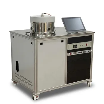
- Inclined Rotary Plasma Enhanced Chemical Vapor Deposition PECVD Equipment Tube Furnace Machine
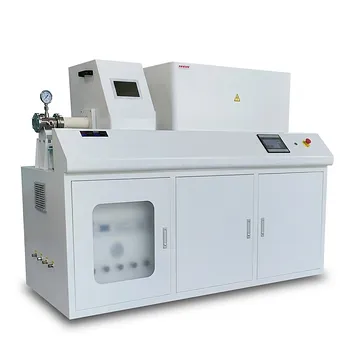
- Chemical Vapor Deposition CVD Equipment System Chamber Slide PECVD Tube Furnace with Liquid Gasifier PECVD Machine
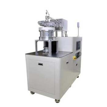
- RF PECVD System Radio Frequency Plasma-Enhanced Chemical Vapor Deposition RF PECVD
- Evaporation Boat for Organic Matter
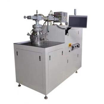
- Microwave Plasma Chemical Vapor Deposition MPCVD Machine System Reactor for Lab and Diamond Growth
People Also Ask
- How are thin films deposited? A Guide to PVD vs. CVD Methods for Your Application
- What are the process capabilities of ICPCVD systems? Achieve Low-Damage Film Deposition at Ultra-Low Temperatures
- What is the process of PECVD in semiconductor? Enabling Low-Temperature Thin Film Deposition
- Why is a Matching Network Indispensable in RF-PECVD for Siloxane Films? Ensure Stable Plasma and Uniform Deposition
- Why does a PECVD vacuum system require both a rotary vane and turbo pump? Ensure High-Purity Coatings
