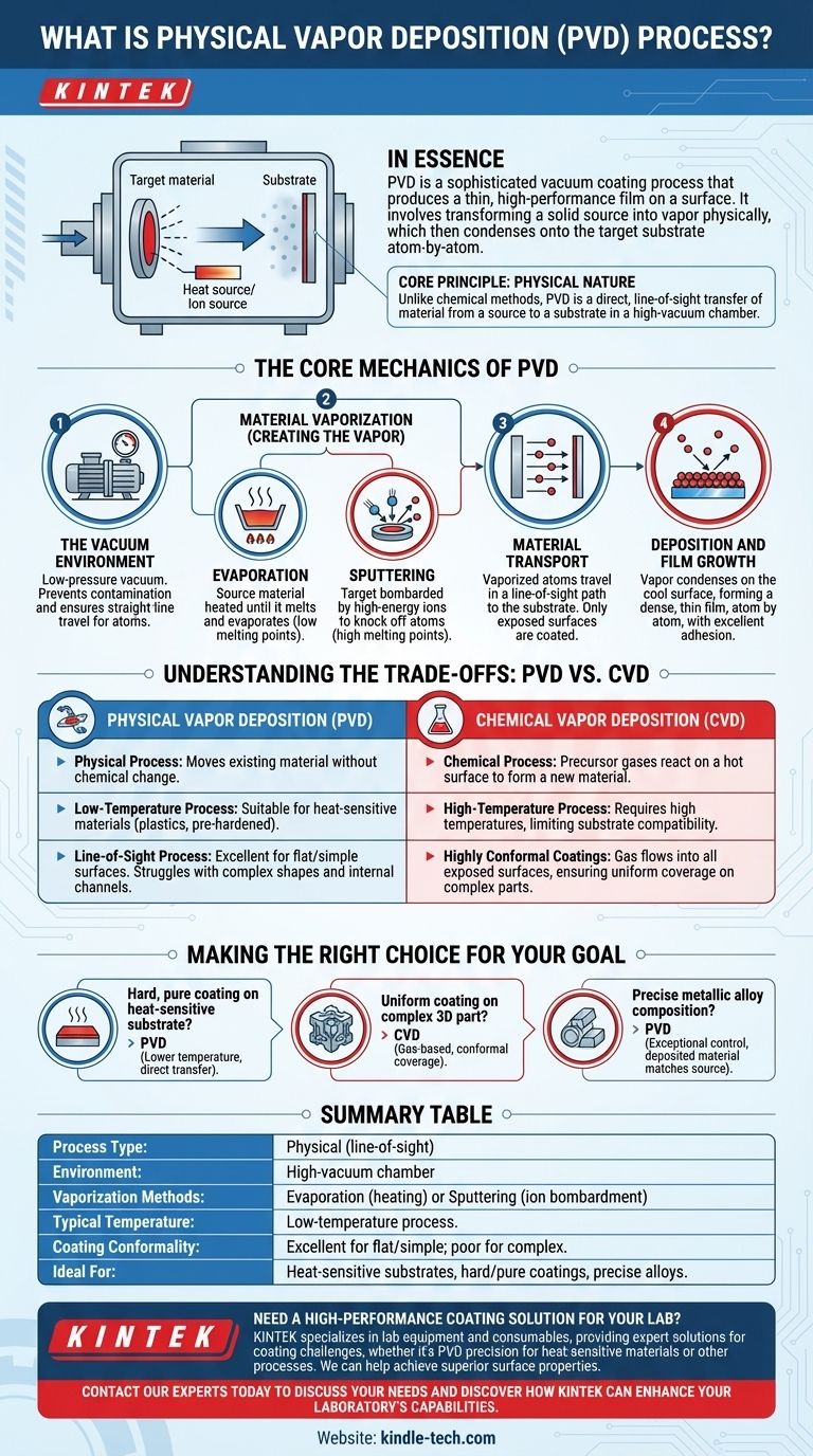
In essence, Physical Vapor Deposition (PVD) is a sophisticated vacuum coating process that produces a thin, high-performance film on a surface. The technique works by taking a solid source material, turning it into a vapor through physical means like heating or ion bombardment, and then allowing this vapor to condense onto the target object, known as the substrate. This atom-by-atom deposition creates an extremely pure and well-adhered coating.
The core principle of PVD is its physical nature. Unlike other methods that rely on chemical reactions, PVD is a direct, line-of-sight transfer of material from a source to a substrate, similar to spray painting on an atomic scale within a high-vacuum chamber.
The Core Mechanics of PVD
The PVD process, while varied, follows a consistent sequence of steps to transform a solid material into a functional coating. Each stage is critical for the final quality of the film.
The Vacuum Environment
The entire PVD process occurs under a very low-pressure vacuum. This is non-negotiable for two reasons.
First, it removes atmospheric gases that could contaminate the coating and introduce impurities. Second, it ensures the vaporized material atoms can travel from the source to the substrate without colliding with air molecules.
Material Vaporization (Creating the Vapor)
To deposit a material, it must first be turned into a vapor. PVD achieves this primarily through two methods.
- Evaporation: The source material is heated in the vacuum chamber until it melts and evaporates, releasing atoms into the chamber. This is effective for materials with lower melting points.
- Sputtering: The source material (or "target") is bombarded with high-energy ions, typically from an inert gas like argon. These collisions have enough force to physically knock atoms off the target, launching them toward the substrate. Sputtering is ideal for materials with very high melting points.
Material Transport
Once vaporized, the material atoms travel in a straight line from the source to the substrate. This is why PVD is often called a "line-of-sight" process. The parts of the substrate directly facing the source get coated, while hidden or shadowed areas do not.
Deposition and Film Growth
When the vaporized atoms strike the cooler surface of the substrate, they condense back into a solid state. They arrange themselves layer by layer, forming a dense, thin film that grows atom by atom. This method results in excellent adhesion between the coating and the substrate.
Understanding the Trade-offs: PVD vs. CVD
To truly understand PVD, it is useful to contrast it with its common alternative, Chemical Vapor Deposition (CVD). While both produce thin films, their mechanisms are fundamentally different.
The Key Distinction: Physical vs. Chemical
PVD is a physical process. It moves existing material from a source to a substrate without changing its chemical composition.
CVD is a chemical process. It introduces precursor gases into a chamber, which then react on the hot surface of the substrate to form an entirely new solid material as the coating.
Temperature and Substrate Compatibility
PVD is a comparatively low-temperature process. This makes it suitable for coating materials that cannot withstand high heat, such as plastics, certain alloys, or pre-hardened components.
CVD typically requires very high temperatures to drive the necessary chemical reactions. This limits its use to substrates that are thermally stable and will not be damaged by the heat.
Coating Properties and Conformality
Because PVD is a line-of-sight process, it is excellent for coating flat or simply curved surfaces. It struggles, however, to uniformly coat complex shapes with internal channels or undercuts.
CVD excels at creating highly conformal coatings. Because the precursor is a gas, it can flow into and react on all exposed surfaces of a complex part, providing a uniform coating thickness everywhere.
Making the Right Choice for Your Goal
The decision between PVD and other coating methods depends entirely on the material, the geometry of the part, and the desired final properties.
- If your primary focus is a hard, pure coating on a heat-sensitive substrate: PVD is the superior choice due to its lower process temperature and direct material transfer.
- If your primary focus is to uniformly coat a complex 3D part with intricate geometry: CVD is the better option because its gas-based process ensures complete, conformal coverage.
- If your primary focus is depositing a metallic alloy with precise composition: PVD provides exceptional control, as the deposited material is the same as the source material.
By understanding the fundamental physical mechanism of PVD, you can confidently select the right tool to achieve your desired surface properties.
Summary Table:
| PVD Aspect | Key Detail |
|---|---|
| Process Type | Physical (line-of-sight material transfer) |
| Environment | High-vacuum chamber |
| Vaporization Methods | Evaporation (heating) or Sputtering (ion bombardment) |
| Typical Temperature | Low-temperature process |
| Coating Conformality | Excellent for flat/simple surfaces; poor for complex geometries |
| Ideal For | Heat-sensitive substrates, hard/pure coatings, precise alloy deposition |
Need a high-performance coating solution for your lab?
KINTEK specializes in lab equipment and consumables, providing expert solutions for your coating challenges. Whether you require the precision of PVD for heat-sensitive materials or need guidance on the best process for your application, our team is here to help.
We can help you achieve superior surface properties with the right equipment. Contact our experts today to discuss your specific needs and discover how KINTEK can enhance your laboratory's capabilities.
Visual Guide
Related Products
- Chemical Vapor Deposition CVD Equipment System Chamber Slide PECVD Tube Furnace with Liquid Gasifier PECVD Machine
- RF PECVD System Radio Frequency Plasma-Enhanced Chemical Vapor Deposition RF PECVD
- 915MHz MPCVD Diamond Machine Microwave Plasma Chemical Vapor Deposition System Reactor
- HFCVD Machine System Equipment for Drawing Die Nano-Diamond Coating
- Split Chamber CVD Tube Furnace with Vacuum Station Chemical Vapor Deposition System Equipment Machine
People Also Ask
- How are carbon nanotubes grown? Master Scalable Production with Chemical Vapor Deposition
- What types of substrates are used in CVD to facilitate graphene films? Optimize Graphene Growth with the Right Catalyst
- Why is Chemical Vapor Deposition (CVD) equipment uniquely suited for constructing hierarchical superhydrophobic structures?
- How expensive is chemical vapor deposition? Understanding the True Cost of High-Performance Coating
- What is plasma enhanced chemical vapor deposition PECVD equipment? A Guide to Low-Temperature Thin Film Deposition


