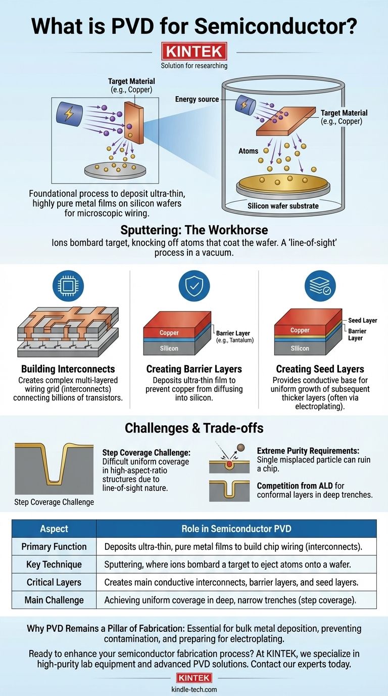
In semiconductor manufacturing, Physical Vapor Deposition (PVD) is a foundational process used to deposit ultra-thin, highly pure metal films onto a silicon wafer. It is not merely a coating for protection; it is a primary method for constructing the microscopic wiring that connects the billions of transistors on a modern chip. The most common form of PVD used in this context is known as sputtering.
At its core, the challenge of chipmaking is creating unimaginably small and precise electrical pathways. PVD is the essential technology that solves this problem by "drawing" these metallic circuits, atom by atom, in a vacuum.
The Fundamental Role of PVD in Chipmaking
To understand PVD's importance, you must see it not as a simple coating process, but as a fundamental construction step. It operates within a vacuum chamber to ensure absolute purity, which is critical for device performance.
What is Physical Vapor Deposition?
Think of PVD as a highly controlled, atomic-level spray-painting process. A solid source material, known as a "target" (e.g., a block of pure copper), is bombarded with energy inside a vacuum chamber. This energy vaporizes the material, ejecting individual atoms or molecules that then travel and deposit onto the cooler silicon wafer, forming an extremely thin and uniform film.
Sputtering: The Workhorse of Semiconductor PVD
The most prevalent PVD technique in chip fabrication is sputtering. In this method, the target material is bombarded with high-energy ions (typically from an inert gas like argon). This collision has a physical impact, "sputtering" or knocking atoms off the target. These ejected atoms then travel in a straight line and coat the wafer's surface.
Building the Interconnects
The primary purpose of PVD in semiconductor manufacturing is to create interconnects. After transistors are formed in the silicon, PVD is used to deposit layers of metal—most commonly copper today, but also tungsten and aluminum—that form the complex, multi-layered wiring grid connecting those transistors. Without these PVD-deposited interconnects, the chip would be nothing more than a collection of isolated switches.
Creating Barrier and Seed Layers
Modern chips require more than just the main conductive metal. To prevent the copper interconnects from "leaking" or diffusing into the silicon and destroying the transistors, a barrier layer is needed. PVD is used to deposit an ultra-thin barrier film (e.g., tantalum or tantalum nitride) before the main copper deposition.
Following that, a thin seed layer of copper is often deposited using PVD. This layer acts as a perfect conductive base to ensure the subsequent, thicker copper layer (often applied via a different process like electroplating) grows with the correct structure and uniformity.
Understanding the Trade-offs and Challenges
While essential, PVD is not without its limitations, especially as chip features shrink to the atomic scale.
The Challenge of Step Coverage
Sputtering is a "line-of-sight" process, meaning the atoms travel in a relatively straight path from the target to the wafer. As the trenches etched into the wafer become deeper and narrower (known as high-aspect-ratio structures), it becomes difficult for the sputtered atoms to uniformly coat the bottom and sidewalls. This can result in a thinner film at the bottom of a trench, which can compromise the circuit's reliability.
Competition from Other Deposition Methods
Because of the step coverage challenge, other technologies are used alongside PVD. Atomic Layer Deposition (ALD), which builds films one atomic layer at a time, offers superior uniformity in deep trenches. However, ALD is significantly slower than PVD. The two are often used together—PVD for speed in bulk deposition and ALD for critical, conformal layers.
Extreme Purity Requirements
The PVD process for semiconductors is unforgiving. Any impurity in the target material or any stray molecules in the vacuum chamber can become embedded in the deposited film. A single misplaced particle can cause a short or open circuit, rendering the entire multi-million dollar chip useless. This necessitates extremely expensive, pure source materials and ultra-high vacuum environments.
Why PVD Remains a Pillar of Fabrication
PVD's role is defined by its unique capabilities for specific, critical tasks within the overall fabrication sequence.
- If your primary focus is bulk metal deposition: PVD sputtering is the industry standard for rapidly and reliably depositing the primary conductive layers of copper, aluminum, or tungsten.
- If your primary focus is preventing contamination: PVD is essential for depositing the thin barrier layers that isolate the conductive metals from the underlying silicon.
- If your primary focus is preparing for electroplating: PVD is used to lay down the critical seed layer that provides a perfect foundation for growing uniform copper interconnects.
Ultimately, PVD is the technology that transforms a patterned silicon wafer into a functioning electronic circuit.
Summary Table:
| Aspect | Role in Semiconductor PVD |
|---|---|
| Primary Function | Deposits ultra-thin, pure metal films to build chip wiring (interconnects). |
| Key Technique | Sputtering, where ions bombard a target to eject atoms onto a wafer. |
| Critical Layers | Creates main conductive interconnects, barrier layers, and seed layers. |
| Main Challenge | Achieving uniform coverage in deep, narrow trenches (step coverage). |
Ready to enhance your semiconductor fabrication process?
At KINTEK, we specialize in providing high-purity lab equipment and consumables, including advanced PVD solutions. Our expertise ensures the reliability and precision your laboratory demands for critical applications like depositing barrier and seed layers.
Contact our experts today to discuss how our PVD systems can meet your specific semiconductor manufacturing needs.
Visual Guide
Related Products
- RF PECVD System Radio Frequency Plasma-Enhanced Chemical Vapor Deposition RF PECVD
- Inclined Rotary Plasma Enhanced Chemical Vapor Deposition PECVD Equipment Tube Furnace Machine
- Chemical Vapor Deposition CVD Equipment System Chamber Slide PECVD Tube Furnace with Liquid Gasifier PECVD Machine
- Microwave Plasma Chemical Vapor Deposition MPCVD Machine System Reactor for Lab and Diamond Growth
- Cylindrical Resonator MPCVD Machine System Reactor for Microwave Plasma Chemical Vapor Deposition and Lab Diamond Growth
People Also Ask
- How does RF power create plasma? Achieve Stable, High-Density Plasma for Your Applications
- What is plasma activated chemical vapour deposition method? A Low-Temperature Solution for Advanced Coatings
- What is an example of PECVD? RF-PECVD for High-Quality Thin Film Deposition
- What is the principle of plasma enhanced chemical vapor deposition? Achieve Low-Temperature Thin Film Deposition
- What are the advantages of PECVD? Enable Low-Temperature, High-Quality Thin-Film Deposition