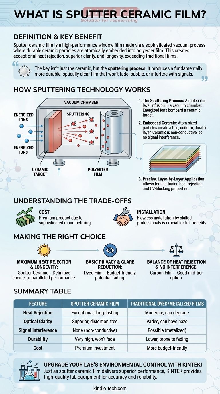
Knowledge What is Sputter Ceramic Film? 5 Key Points Explained
Author avatar

Tech Team · Kintek Solution

Updated 3 weeks ago

What is Sputter Ceramic Film? 5 Key Points Explained

Sputter ceramic film is a high-performance, thin film produced through the sputtering process.

This process involves the deposition of atoms from a solid target material onto a substrate.

Sputtering is widely used in various industries, including electronics, optics, and decorative applications.

It creates films with excellent uniformity, density, purity, and adhesion.

These films can be tailored to specific properties such as reflectivity, electrical resistivity, and thermal insulation.

5 Key Points Explained

What is Sputter Ceramic Film? 5 Key Points Explained

1. Sputtering Process Overview

Sputtering is a vacuum-enabled process where a target material is bombarded with gaseous plasma.

This causes atoms to be dislodged and deposited onto a substrate.

The target and substrate are placed in a vacuum chamber.

A voltage is applied to create a plasma that interacts with the target material.

This process allows for the precise control of film properties such as morphology, grain orientation, and density.

2. Types of Sputtering

Various methods exist, including cathodic sputtering, diode sputtering, RF or DC sputtering, and reactive sputtering.

Each method varies in the specifics of how the plasma is generated and controlled.

Reactive sputtering involves the use of reactive gases to form compounds such as oxides or nitrides on the substrate.

3. Applications of Sputter Ceramic Film

In electronics, sputter films are used for thin film wiring on chips, recording heads, and magnetic media.

In architectural and decorative applications, sputter films provide thermal insulation, wear resistance, and enhanced appearance.

Sputter films are also used in solar cells for transparent electrodes and in the food packaging industry for thin plastic films.

4. Properties and Benefits of Sputter Ceramic Film

The films exhibit excellent uniformity, density, and adhesion, making them durable and long-lasting.

They can be customized to provide specific properties such as heat rejection, electrical conductivity, and optical clarity.

The process is relatively inexpensive compared to other deposition methods, offering a cost-effective solution for various applications.

5. Industry Impact and Future Trends

Sputter ceramic films are integral to modern technology, enhancing performance in semiconductors, optics, and decorative materials.

Continuous advancements in sputtering technology are expected to expand the range of applications and improve the efficiency and quality of sputter films.

In summary, sputter ceramic film is a versatile and high-performance material produced through a controlled vacuum process.

Its ability to be tailored to specific properties and its wide range of applications make it a crucial component in modern technology and industry.

Continue exploring, consult our experts

Unleash the Power of Sputter Ceramic Films with KINTEK SOLUTION!

Discover the precision, versatility, and efficiency that our high-performance films bring to your projects.

Don't miss out on the opportunity to elevate your industry.

Contact KINTEK SOLUTION today to explore how our cutting-edge sputter ceramic films can transform your applications!

Related Products

High Purity Selenium (Se) Sputtering Target / Powder / Wire / Block / Granule

High Purity Selenium (Se) Sputtering Target / Powder / Wire / Block / Granule

Looking for affordable Selenium (Se) materials for laboratory use? We specialize in producing and tailoring materials of various purities, shapes, and sizes to suit your unique requirements. Explore our range of sputtering targets, coating materials, powders, and more.

Silicon Carbide (SiC) Sputtering Target / Powder / Wire / Block / Granule

Silicon Carbide (SiC) Sputtering Target / Powder / Wire / Block / Granule

Looking for high-quality Silicon Carbide (SiC) materials for your lab? Look no further! Our expert team produces and tailors SiC materials to your exact needs at reasonable prices. Browse our range of sputtering targets, coatings, powders, and more today.

Silicon Carbide (SIC) Ceramic Sheet Flat / Corrugated Heat Sink

Silicon Carbide (SIC) Ceramic Sheet Flat / Corrugated Heat Sink

Silicon carbide (sic) ceramic heat sink not only does not generate electromagnetic waves, but also can isolate electromagnetic waves and absorb part of electromagnetic waves.

Aluminized ceramic evaporation boat

Aluminized ceramic evaporation boat

Vessel for depositing thin films; has an aluminum-coated ceramic body for improved thermal efficiency and chemical resistance. making it suitable for various applications.

Aluminum Oxide (Al2O3) Ceramics Heat Sink - Insulation

Aluminum Oxide (Al2O3) Ceramics Heat Sink - Insulation

The hole structure of the ceramic heat sink increases the heat dissipation area in contact with the air, which greatly enhances the heat dissipation effect, and the heat dissipation effect is better than that of super copper and aluminum.

High temperature resistant optical quartz glass sheet

High temperature resistant optical quartz glass sheet

Discover the power of optical glass sheets for precise light manipulation in telecommunications, astronomy, and beyond. Unlock advancements in optical technology with exceptional clarity and tailored refractive properties.

Ceramic Evaporation Boat Set

Ceramic Evaporation Boat Set

It can be used for vapor deposition of various metals and alloys. Most metals can be evaporated completely without loss. Evaporation baskets are reusable.1

Vacuum pressure sintering furnace

Vacuum pressure sintering furnace

Vacuum pressure sintering furnaces are designed for high temperature hot pressing applications in metal and ceramic sintering. Its advanced features ensure precise temperature control, reliable pressure maintenance, and a robust design for seamless operation.

High Purity Cerium (Ce) Sputtering Target / Powder / Wire / Block / Granule

High Purity Cerium (Ce) Sputtering Target / Powder / Wire / Block / Granule

Looking for high-quality Cerium (Ce) materials for your laboratory? Our expertise lies in producing and tailoring materials of different purities, shapes, and sizes to suit your unique requirements. We offer a range of specifications and sizes, including sputtering targets, coating materials, powders, and more, all at reasonable prices.

Optical ultra-clear glass sheet for laboratory K9 / B270 / BK7

Optical ultra-clear glass sheet for laboratory K9 / B270 / BK7

Optical glass, while sharing many characteristics with other types of glass, is manufactured using specific chemicals that enhance properties crucial for optics applications.

Silicon Carbide (SIC) Ceramic Plate

Silicon Carbide (SIC) Ceramic Plate

Silicon nitride (sic) ceramic is an inorganic material ceramic that does not shrink during sintering. It is a high-strength, low-density, high-temperature-resistant covalent bond compound.

Optical quartz plate JGS1 / JGS2 / JGS3

Optical quartz plate JGS1 / JGS2 / JGS3

The quartz plate is a transparent, durable, and versatile component widely used in various industries. Made from high-purity quartz crystal, it exhibits excellent thermal and chemical resistance.

Plasma enhanced evaporation deposition PECVD coating machine

Plasma enhanced evaporation deposition PECVD coating machine

Upgrade your coating process with PECVD coating equipment. Ideal for LED, power semiconductors, MEMS and more. Deposits high-quality solid films at low temps.

9MPa air pressure sintering furnace

9MPa air pressure sintering furnace

The air pressure sintering furnace is a high-tech equipment commonly used for the sintering of advanced ceramic materials. It combines vacuum sintering and pressure sintering techniques to achieve high-density and high-strength ceramics.

Cerium Fluoride (CeF3) Sputtering Target / Powder / Wire / Block / Granule

Cerium Fluoride (CeF3) Sputtering Target / Powder / Wire / Block / Granule

Looking for high-quality Cerium Fluoride materials? Our lab-grade CeF3 is available in a variety of shapes and sizes to meet your needs. Shop now for affordable prices!

Optical Windows

Optical Windows

Diamond optical windows: exceptional broad band infrared transparency, excellent thermal conductivity & low scattering in infrared, for high-power IR laser & microwave windows applications.

Spark plasma sintering furnace SPS furnace

Spark plasma sintering furnace SPS furnace

Discover the benefits of Spark Plasma Sintering Furnaces for rapid, low-temperature material preparation. Uniform heating, low cost & eco-friendly.

Float soda-lime optical glass for laboratory

Float soda-lime optical glass for laboratory

Soda-lime glass, widely favored as an insulating substrate for thin/thick film deposition, is created by floating molten glass on molten tin. This method ensures uniform thickness and exceptionally flat surfaces.

Silicon Carbide (SIC) Ceramic Sheet Wear-Rresistant

Silicon Carbide (SIC) Ceramic Sheet Wear-Rresistant

Silicon carbide (sic) ceramic sheet is composed of high-purity silicon carbide and ultra-fine powder, which is formed by vibration molding and high-temperature sintering.

Electron Beam Evaporation Coating Oxygen-Free Copper Crucible

Electron Beam Evaporation Coating Oxygen-Free Copper Crucible

Electron Beam Evaporation Coating Oxygen-Free Copper Crucible enables precise co-deposition of various materials. Its controlled temperature and water-cooled design ensure pure and efficient thin film deposition.

915MHz MPCVD Diamond Machine

915MHz MPCVD Diamond Machine

915MHz MPCVD Diamond Machine and its multi-crystal effective growth, the maximum area can reach 8 inches, the maximum effective growth area of single crystal can reach 5 inches. This equipment is mainly used for the production of large-size polycrystalline diamond films, the growth of long single crystal diamonds, the low-temperature growth of high-quality graphene, and other materials that require energy provided by microwave plasma for growth.

CVD boron doped diamond

CVD boron doped diamond

CVD boron-doped diamond: A versatile material enabling tailored electrical conductivity, optical transparency, and exceptional thermal properties for applications in electronics, optics, sensing, and quantum technologies.

Small vacuum tungsten wire sintering furnace

Small vacuum tungsten wire sintering furnace

The small vacuum tungsten wire sintering furnace is a compact experimental vacuum furnace specially designed for universities and scientific research institutes. The furnace features a CNC welded shell and vacuum piping to ensure leak-free operation. Quick-connect electrical connections facilitate relocation and debugging, and the standard electrical control cabinet is safe and convenient to operate.

Hemispherical Bottom Tungsten / Molybdenum Evaporation Boat

Hemispherical Bottom Tungsten / Molybdenum Evaporation Boat

Used for gold plating, silver plating, platinum, palladium, suitable for a small amount of thin film materials. Reduce the waste of film materials and reduce heat dissipation.

CaF2 substrate / window / lens

CaF2 substrate / window / lens

A CaF2 window is an optical window made of crystalline calcium fluoride. These windows are versatile, environmentally stable and resistant to laser damage, and they exhibit a high, stable transmission from 200 nm to about 7 μm.

High Purity Antimony (Sb) Sputtering Target / Powder / Wire / Block / Granule

High Purity Antimony (Sb) Sputtering Target / Powder / Wire / Block / Granule

Get high-quality Antimony (Sb) materials tailored to your specific needs. We offer a wide range of shapes and sizes at reasonable prices. Browse our sputtering targets, powders, foils, and more.


Leave Your Message