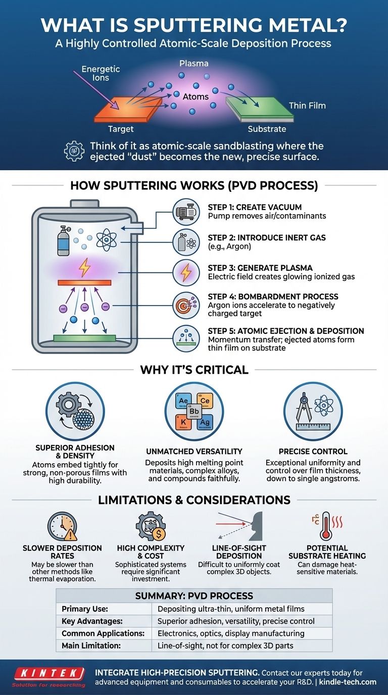
At its core, sputtering is a highly controlled process for depositing an ultra-thin layer of metal onto a surface. It works by ejecting atoms from a source material, called a "target," by bombarding it with energetic ions in a vacuum. These ejected atoms then travel and condense on a substrate—such as a silicon wafer, glass, or plastic—forming a uniform and high-quality thin film.
Sputtering is best understood not as painting or plating, but as a form of atomic-scale sandblasting where the ejected "dust" becomes the new surface. This physical process gives engineers and scientists precise control over film thickness, purity, and density, making it essential for manufacturing high-performance modern electronics.
How Sputtering Works: From Plasma to Thin Film
Sputtering is a type of physical vapor deposition (PVD). The entire process takes place inside a sealed, low-pressure vacuum chamber to ensure the purity of the final film.
Step 1: Creating a Vacuum
First, the chamber is pumped down to a high vacuum. This removes air and other particles that could contaminate the metal film or interfere with the process.
Step 2: Introducing an Inert Gas
A small, precisely controlled amount of an inert gas, typically Argon (Ar), is then introduced into the chamber. This gas is not reactive and will not chemically bond with the metal.
Step 3: Generating a Plasma
A strong electric field is applied within the chamber. This field energizes the argon gas, stripping electrons from the argon atoms and creating a glowing, ionized gas known as a plasma. This plasma is a mixture of positively charged argon ions and free electrons.
Step 4: The Bombardment Process
The metal to be deposited, known as the target, is given a strong negative electrical charge. The positively charged argon ions in the plasma are naturally attracted to and accelerate towards the negatively charged target, striking its surface with significant force.
Step 5: Atomic Ejection and Deposition
Each collision is a pure momentum transfer event. Think of a fast-moving cue ball (the argon ion) hitting a rack of billiard balls (the metal atoms of the target). The impact has enough energy to knock individual atoms completely free from the target material.
These "sputtered" metal atoms then travel in a straight line through the vacuum until they strike the substrate, which is strategically placed to intercept them. Atom by atom, they build up on the substrate, forming a thin, dense, and highly uniform film.
Why Sputtering is a Critical Technology
Sputtering is not always the fastest or cheapest deposition method, but it is chosen when the quality and properties of the final film are paramount.
Superior Film Adhesion and Density
Because the sputtered atoms arrive at the substrate with significant kinetic energy, they embed themselves tightly into the surface. This creates films with exceptionally strong adhesion and a dense, non-porous structure, which is critical for durability and performance.
Unmatched Material Versatility
Unlike thermal evaporation, which relies on melting materials, sputtering is a mechanical process. This means it can be used to deposit materials with extremely high melting points, such as tungsten and tantalum, as well as complex alloys and compounds. The composition of an alloy target is faithfully reproduced in the deposited film.
Precise Control and Uniformity
The sputtering process offers exceptional control over film thickness, often down to the single-angstrom level (less than the diameter of an atom). By carefully managing gas pressure, power, and time, engineers can produce highly uniform films over very large areas, such as architectural glass or flat-panel displays.
Understanding the Trade-offs and Limitations
While powerful, sputtering has specific drawbacks that make it unsuitable for certain applications.
Slower Deposition Rates
Generally, sputtering deposits material more slowly than other methods like thermal evaporation. For applications where speed is the priority and film quality is less critical, sputtering can be a bottleneck.
High System Complexity and Cost
Sputtering systems are sophisticated and expensive. They require high-vacuum pumps, powerful electrical supplies, complex gas handling, and often, advanced cooling systems. This represents a significant capital investment.
Line-of-Sight Deposition
Sputtered atoms travel in a straight line from the target to the substrate. This makes it difficult to uniformly coat complex, three-dimensional objects with shadowed areas or internal surfaces.
Potential Substrate Heating
The energy transfer from the condensing atoms can heat the substrate. While this can sometimes be beneficial for film quality, it can damage heat-sensitive substrates like certain plastics or biological materials.
Making the Right Choice for Your Goal
Sputtering is an essential tool, but its use must be justified by your project's technical demands.
- If your primary focus is high-purity, dense films for advanced electronics or optics: Sputtering is the industry standard for creating semiconductor interconnects, anti-reflection coatings, and other high-performance layers.
- If your primary focus is rapid, low-cost coating of simple metals: Thermal evaporation is often a more economical choice for applications like decorative chrome on plastic or aluminum on reflectors.
- If your primary focus is coating complex 3D parts uniformly: You should investigate non-line-of-sight methods like atomic layer deposition (ALD) or chemical vapor deposition (CVD).
Ultimately, understanding the principles of sputtering empowers you to select the precise tool needed to build materials from the atom up.
Summary Table:
| Aspect | Key Point |
|---|---|
| Process Type | Physical Vapor Deposition (PVD) |
| Primary Use | Depositing ultra-thin, uniform metal films |
| Key Advantages | Superior film adhesion, material versatility, precise thickness control |
| Common Applications | Semiconductor interconnects, anti-reflection coatings, display manufacturing |
| Main Limitation | Line-of-sight deposition, not ideal for complex 3D parts |
Ready to integrate high-precision sputtering into your lab's workflow?
KINTEK specializes in providing advanced lab equipment and consumables for all your thin-film deposition needs. Whether you are developing next-generation electronics, optical coatings, or specialized materials, our expertise and solutions ensure superior film quality, adhesion, and performance.
Contact our experts today to discuss how our sputtering systems and support can accelerate your research and development.
Visual Guide
Related Products
- Spark Plasma Sintering Furnace SPS Furnace
- Vacuum Induction Melting Spinning System Arc Melting Furnace
- Chemical Vapor Deposition CVD Equipment System Chamber Slide PECVD Tube Furnace with Liquid Gasifier PECVD Machine
- Customer Made Versatile CVD Tube Furnace Chemical Vapor Deposition Chamber System Equipment
People Also Ask
- What are the advantages of CAMI/SPS for W-Cu composite preparation? Reduce cycles from hours to seconds.
- What is the mechanism of SPS process? A Deep Dive into Rapid, Low-Temperature Sintering
- Why are Spark Plasma Sintering (SPS) furnaces or hot presses utilized in the preparation of Li3PS4 solid electrolytes?
- What is the process fundamentals of spark plasma sintering? Achieve Rapid, High-Density Material Consolidation
- What are the fundamentals of spark plasma sintering process? Unlock Rapid, High-Performance Material Consolidation


