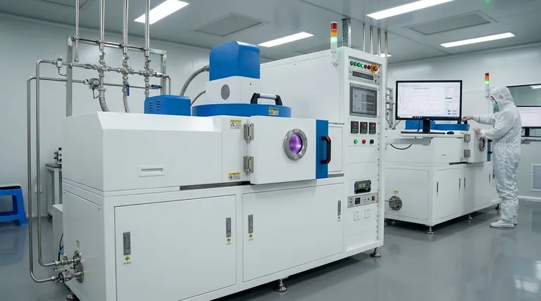
In essence, magnetron sputtering is a highly controlled vacuum deposition technique used to create extremely thin and uniform films of material. It works by creating a plasma, accelerating ions from that plasma to physically chip atoms off a source material (the "target"), and then depositing those atoms onto a substrate. The "magnetron" part refers to the critical use of a magnetic field to dramatically increase the efficiency and speed of this process.
The central principle of magnetron sputtering is not just the bombardment of a target, but the strategic use of a magnetic field to trap electrons near the target's surface. This confinement creates a dense, localized plasma, which significantly increases the rate of atom ejection and allows for faster, more controlled thin-film deposition at lower pressures.
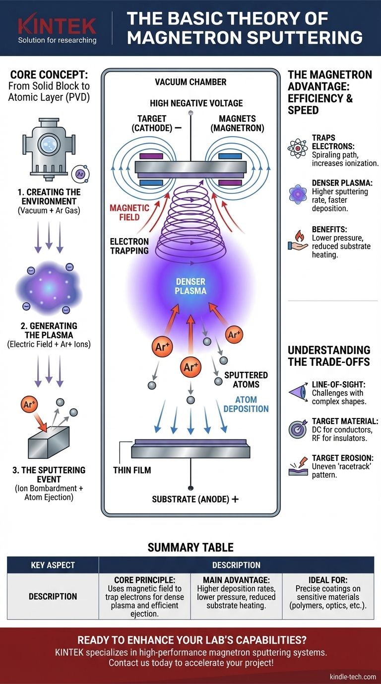
The Core Concept: From Solid Block to Atomic Layer
Physical Vapor Deposition (PVD) is a category of processes where a solid material is vaporized in a vacuum and condensed onto a surface as a thin film. Sputtering is a specific type of PVD that achieves this through physical momentum transfer, much like a sandblaster precisely chipping away at a surface, but on an atomic scale.
Step 1: Creating the Environment
The entire process occurs inside a high-vacuum chamber. This is critical to ensure the sputtered atoms can travel from the target to the substrate without colliding with unwanted air molecules, which would contaminate the film.
Once a vacuum is achieved, a small, precisely controlled amount of an inert gas, typically Argon (Ar), is introduced into the chamber. This gas provides the atoms that will be ionized to create the plasma.
Step 2: Generating the Plasma
A high negative voltage is applied to the target material, making it a cathode. The chamber walls or a separate electrode act as the anode. This voltage differential creates a powerful electric field.
This field energizes free electrons in the chamber, causing them to accelerate and collide with the neutral Argon atoms. These collisions knock electrons off the Argon atoms, creating positively charged Argon ions (Ar+). This self-sustaining cloud of ions and electrons is the plasma, which often emits a characteristic colorful glow known as a glow discharge.
Step 3: The Sputtering Event
The positively charged Ar+ ions are powerfully attracted to the negatively charged target. They accelerate across the electric field and violently collide with the target's surface.
Each impact is energetic enough to transfer momentum that ejects, or "sputters," individual atoms from the target material. These ejected atoms are neutral and travel in a straight line away from the target. The impact also releases secondary electrons from the target, which are crucial for the next step.
The "Magnetron" Advantage: Why the Magnetic Field is Critical
Without a magnetic field, the process (known as diode sputtering) is slow and inefficient. The addition of a magnetron—a specific arrangement of magnets placed behind the target—revolutionizes the process.
Trapping Electrons for Higher Efficiency
The magnetic field is designed to be strongest near the face of the target. This field traps the secondary electrons that are released during ion bombardment, forcing them into a spiral, or cycloidal, path.
Instead of escaping directly to the anode, these electrons travel a much longer distance within the plasma, right in front of the target. This dramatically increases the probability that they will collide with and ionize more neutral Argon atoms.
The Result: A Denser Plasma and Faster Deposition
This electron-trapping effect creates a far denser, more intense plasma confined to the region directly in front of the target.
A denser plasma means there are many more Ar+ ions available to bombard the target. This leads directly to a much higher sputtering rate, meaning atoms are ejected more quickly and the film deposits much faster.
The Benefit: Lower Pressure and Temperature
Because the magnetic field makes the ionization process so efficient, magnetron sputtering can operate at much lower gas pressures than diode sputtering. This improves the quality of the resulting film, as sputtered atoms encounter fewer gas collisions on their way to the substrate.
Furthermore, by confining the high-energy electrons near the target, the magnetron prevents them from bombarding and heating the substrate. This makes the process suitable for coating heat-sensitive materials like plastics and polymers.
Understanding the Trade-offs
While powerful, magnetron sputtering is not without its limitations. Objectively understanding these is key to its proper application.
Line-of-Sight Deposition
Sputtering is a "line-of-sight" process. Atoms travel in a relatively straight path from the target to the substrate. Coating complex, three-dimensional shapes with a uniform thickness can be challenging and may require sophisticated substrate rotation.
Target Material and Power Source
The most common configuration, Direct Current (DC) sputtering, requires the target material to be electrically conductive. Coating insulating or ceramic materials requires the use of a more complex and expensive Radio Frequency (RF) power supply.
Target Erosion and Utilization
The magnetic field that enhances the process also concentrates the plasma in a specific area, often in a "racetrack" pattern on the target's surface. This leads to uneven erosion of the target material, meaning not all of the expensive source material can be used before the target must be replaced.
Making the Right Choice for Your Goal
Understanding the core theory allows you to see where this technology excels.
- If your primary focus is high-quality, dense films for optics or electronics: Magnetron sputtering offers exceptional control over film properties like thickness, purity, and density.
- If your primary focus is rapid, industrial-scale coating: The high deposition rates make it a leading choice for coating large areas quickly, such as in architectural glass or semiconductor manufacturing.
- If your primary focus is coating temperature-sensitive substrates: The process inherently minimizes heat transfer to the substrate, making it ideal for polymers, plastics, and other delicate materials.
Magnetron sputtering is a foundational technology in modern manufacturing, enabling the precise engineering of surfaces for countless advanced applications.
Summary Table:
| Key Aspect | Description |
|---|---|
| Core Principle | Uses a magnetic field to trap electrons, creating a dense plasma for efficient atom ejection from a target material. |
| Main Advantage | Higher deposition rates, lower operating pressures, and reduced substrate heating compared to standard sputtering. |
| Ideal For | Applications requiring precise, high-quality coatings on sensitive materials like polymers, semiconductors, and optical components. |
Ready to enhance your lab's capabilities with precise thin-film deposition? KINTEK specializes in high-performance magnetron sputtering systems and lab equipment tailored for research and industrial applications. Whether you're working with sensitive polymers, advanced electronics, or optical coatings, our solutions deliver uniform, high-purity films with exceptional control. Contact us today to discuss how our expertise can accelerate your project and achieve superior results!
Visual Guide
Related Products
- Spark Plasma Sintering Furnace SPS Furnace
- RF PECVD System Radio Frequency Plasma-Enhanced Chemical Vapor Deposition RF PECVD
People Also Ask
- What is the pressure for spark plasma sintering? A Guide to Optimizing SPS Parameters
- What is the theory of spark plasma sintering? A Guide to Rapid, Low-Temperature Densification
- What technical advantages does a Spark Plasma Sintering (SPS) furnace offer for LZP ceramics? Enhance Ionic Conductivity
- What are the advantages of CAMI/SPS for W-Cu composite preparation? Reduce cycles from hours to seconds.
- Why are Spark Plasma Sintering (SPS) furnaces or hot presses utilized in the preparation of Li3PS4 solid electrolytes?

