For producing large-area, high-quality graphene suitable for electronics and commercial applications, Chemical Vapor Deposition (CVD) is widely considered the best and most promising synthesis method. It involves growing a thin film of graphene on a metal catalyst substrate, a process that uniquely combines scalability with excellent material quality.
The "best" method for synthesizing graphene is not a single answer but a strategic choice based on your goal. While Chemical Vapor Deposition (CVD) offers the premier balance of quality and scale for industrial use, other methods like exfoliation are superior for specific research or bulk production scenarios.
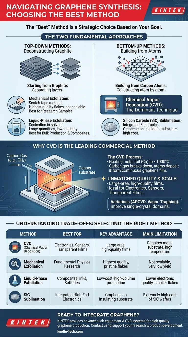
The Two Fundamental Approaches to Graphene Synthesis
Understanding graphene production begins with recognizing the two primary strategies. Each approach starts from a different point and is suited for different end goals.
Top-Down Methods: Starting from Graphite
This approach involves taking bulk graphite—essentially a stack of countless graphene layers—and separating it into individual or few-layer sheets. It is a process of deconstruction.
The most famous example is mechanical exfoliation, the original "Scotch tape" method used to first isolate graphene. It yields extremely high-quality flakes but is not scalable.
Another key method is liquid-phase exfoliation, where graphite is sonicated in a liquid to break it apart. This can produce large quantities of graphene flakes, but the quality is generally lower.
Bottom-Up Methods: Building from Carbon Atoms
This approach constructs graphene atom-by-atom on a suitable substrate. It is a process of creation, offering precise control over the final material.
Chemical Vapor Deposition (CVD) is the dominant bottom-up technique. Other methods in this category include the sublimation of silicon carbide (SiC) and arc discharge, but CVD has emerged as the leader for most practical applications.
Why Chemical Vapor Deposition (CVD) is the Leading Method
CVD has become the most common and celebrated approach because it uniquely solves the dual challenge of achieving both high quality and large area, which is essential for commercial viability.
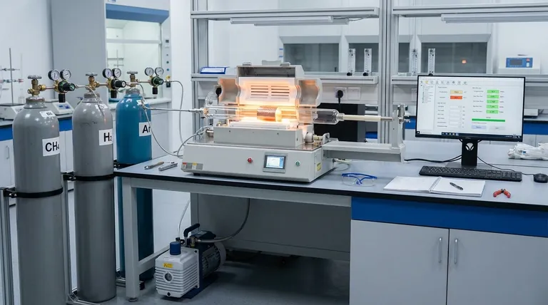
The CVD Process Explained
In a typical CVD process, a metal foil substrate, most commonly copper (Cu), is heated to a high temperature (around 1000°C) inside a furnace.
A carbon-containing gas, such as methane (CH4), is then introduced. The high temperature breaks down the gas, and carbon atoms deposit onto the surface of the metal foil, arranging themselves into the characteristic hexagonal lattice of a single graphene layer.
Unmatched Quality and Scale
The primary advantage of CVD is its ability to grow a continuous, single-layer graphene film over large areas—currently up to wafer-scale dimensions.
This combination of large-area coverage and high electronic quality makes CVD-grown graphene the ideal candidate for applications in transparent conductive films, transistors, sensors, and other advanced electronics.
Variations for Specific Needs
Researchers have developed specialized CVD techniques to further improve quality. Methods like Atmospheric Pressure CVD (APCVD) and the vapor-trapping method are designed to grow larger single-crystal graphene domains, minimizing the defects that can occur at the boundaries between crystals.
Understanding the Trade-offs: When Other Methods are "Best"
While CVD is the leader for high-tech applications, its dominance is not absolute. The "best" method is always relative to the specific requirements of the project, especially regarding cost, scale, and acceptable quality.
Mechanical Exfoliation: For Pristine Research Samples
For fundamental physics research, a single, structurally perfect flake of graphene is often required. Mechanical exfoliation is still the gold standard for producing these pristine samples.
The trade-off is that it is a purely manual, low-yield process that is completely unsuitable for any form of mass production.
Liquid-Phase Exfoliation: For Bulk Production and Composites
When the primary goal is producing a large volume of graphene at a low cost, liquid-phase exfoliation is the superior choice. The output is typically a dispersion of graphene flakes in a solvent.
This material is not suitable for high-end electronics due to smaller flake sizes and more defects. However, it is ideal for applications like conductive inks, polymer composites, coatings, and battery additives, where bulk properties are more important than pristine atomic structure.
Silicon Carbide (SiC) Sublimation: For Integrated High-End Electronics
This method involves heating a silicon carbide wafer to very high temperatures, causing silicon atoms to sublimate (turn into a gas) from the surface, leaving behind a layer of carbon atoms that form graphene.
Its key advantage is that the graphene is grown directly on an insulating substrate, which can simplify device fabrication. The primary trade-off is the extremely high cost of SiC wafers, limiting its use to specialized, high-performance applications.
Selecting the Right Method for Your Application
Your choice of synthesis method must be guided by your ultimate goal. There is no single "best" method, only the one most appropriate for your application's constraints on quality, scale, and cost.
- If your primary focus is high-performance electronics: Chemical Vapor Deposition (CVD) is the clear choice for its balance of large-area coverage and excellent electronic quality.
- If your primary focus is fundamental scientific research: Mechanical exfoliation remains the best method for obtaining the most pristine, defect-free graphene flakes.
- If your primary focus is mass production for composites or inks: Liquid-phase exfoliation provides the most scalable and cost-effective route to producing bulk quantities of graphene.
Understanding these core trade-offs allows you to select not just a method, but the right strategy for your specific goal.
Summary Table:
| Method | Best For | Key Advantage | Main Limitation |
|---|---|---|---|
| Chemical Vapor Deposition (CVD) | Electronics, Sensors, Transparent Films | Large-area, high-quality films | Requires metal substrate, high temperature |
| Mechanical Exfoliation | Fundamental Physics Research | Highest quality, pristine flakes | Not scalable, very low yield |
| Liquid-Phase Exfoliation | Composites, Inks, Batteries | Low-cost, high-volume production | Lower electronic quality, smaller flakes |
| Silicon Carbide (SiC) Sublimation | Integrated High-Performance Electronics | Graphene on insulating substrate | Extremely high cost of SiC wafers |
Ready to Integrate Graphene into Your Research or Product Development?
The right synthesis method is just the beginning. KINTEK specializes in providing the advanced lab equipment, including CVD systems and consumables, needed to successfully produce high-quality graphene for your specific application—whether for cutting-edge electronics, composite materials, or fundamental research.
Let our experts help you build a reliable and efficient synthesis workflow. Contact our team today to discuss your project requirements and discover how KINTEK can support your laboratory's innovation in graphene technology.
Visual Guide
Related Products
- Chemical Vapor Deposition CVD Equipment System Chamber Slide PECVD Tube Furnace with Liquid Gasifier PECVD Machine
- Customer Made Versatile CVD Tube Furnace Chemical Vapor Deposition Chamber System Equipment
- Multi Heating Zones CVD Tube Furnace Machine Chemical Vapor Deposition Chamber System Equipment
- Microwave Plasma Chemical Vapor Deposition MPCVD Machine System Reactor for Lab and Diamond Growth
- HFCVD Machine System Equipment for Drawing Die Nano-Diamond Coating
People Also Ask
- What types of substrates are used in CVD to facilitate graphene films? Optimize Graphene Growth with the Right Catalyst
- What are the advantages of chemical vapor deposition? Achieve Superior Thin Films for Your Lab
- What happens during deposition chemistry? Building Thin Films from Gaseous Precursors
- How are carbon nanotubes grown? Master Scalable Production with Chemical Vapor Deposition
- What are the processes of vapor phase deposition? Understand CVD vs. PVD for Superior Thin Films