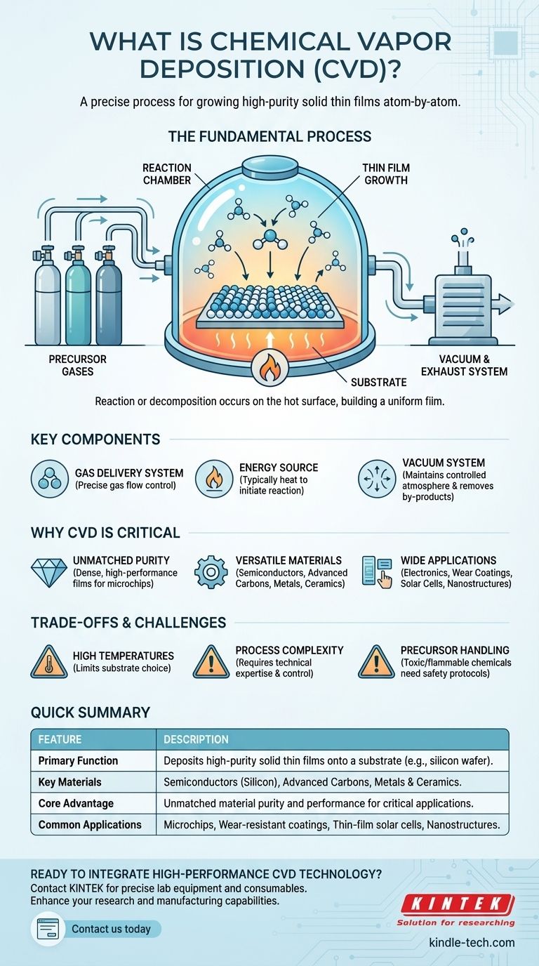
Chemical Vapor Deposition (CVD) is a highly controlled manufacturing process used to grow a high-purity, solid thin film onto a surface, known as a substrate. It works by introducing reactive gases (precursors) into a chamber, which then chemically react or decompose at the substrate's surface, leaving behind a layer of the desired material. This method is fundamental to the production of modern electronics and advanced materials.
CVD is not simply a coating technique; it is a precise chemical synthesis process that occurs directly on a surface. This allows for the atom-by-atom construction of high-performance films, making it an essential technology for the semiconductor, aerospace, and materials science industries.
How Chemical Vapor Deposition Fundamentally Works
To understand CVD, it's best to think of it as building a material from its chemical ingredients in a highly controlled environment. The process relies on several key components and a precise sequence of events.
The Core Components of a CVD System
A typical CVD system consists of a reaction chamber where the deposition takes place. A gas delivery system precisely introduces one or more volatile precursor gases into the chamber. An energy source (often heat) provides the necessary energy to initiate the chemical reaction, while a vacuum system removes air and maintains a controlled atmosphere. Finally, an exhaust system safely handles anp.y volatile by-products generated during the process.
The Deposition Process Explained
First, the substrate—the object to be coated, such as a silicon wafer—is placed inside the reaction chamber. The chamber is then vacuum-sealed to remove any contaminants.
Next, specific precursor gases containing the elements of the desired film are introduced. Energy is applied, typically by heating the substrate, which causes the gases to react or decompose on the hot surface.
This chemical reaction results in a solid material being deposited, forming a thin film that grows layer by layer on the substrate. Any gaseous by-products from the reaction are continuously removed from the chamber by the gas flow and exhaust system.
What Makes CVD a Critical Technology?
CVD's widespread use stems from its ability to produce materials with exceptional quality and versatility, which is impossible to achieve with many other methods.
Unmatched Purity and Performance
Because the process occurs in a controlled vacuum environment with highly pure precursor gases, CVD can produce extremely dense, high-purity films. This results in materials with superior electrical, optical, and mechanical properties, which are critical for high-performance applications like microchips.
Versatility of Materials and Substrates
CVD is incredibly versatile. It can be used to deposit a vast range of materials, including:
- Semiconductors: Silicon, silicon nitride, silicon dioxide
- Advanced Carbons: Diamond, graphene, carbon nanotubes, and nanofibers
- Metals & Ceramics: Tungsten, titanium nitride, and various high-k dielectrics
This process can be applied to many different substrates, including metals, ceramics, and glass, making it adaptable across numerous industries.
Wide-Ranging Industrial Applications
This versatility allows CVD to be a cornerstone technology in several key sectors. It is used for depositing thin films on semiconductors in electronics, creating wear- and corrosion-resistant coatings for cutting tools, and depositing photovoltaic materials for thin-film solar cells.
Understanding the Trade-offs and Challenges
While powerful, CVD is a complex process with specific requirements and limitations that must be considered.
Requirement for High Temperatures
Traditional CVD processes often require very high temperatures to drive the chemical reactions. This can limit the types of substrate materials that can be used, as some may not be able to withstand the heat without deforming or melting.
Process Complexity and Expertise
Operating CVD equipment requires a high level of technical skill and process control. Factors like temperature, pressure, gas flow rates, and chemistry must be meticulously managed to achieve a uniform, high-quality film. This complexity increases both equipment and operational costs.
Handling of Precursor Chemicals
The precursor gases used in CVD can be highly toxic, flammable, or corrosive. This necessitates sophisticated safety protocols, gas handling systems, and exhaust treatment to ensure safe operation and mitigate environmental impact.
Making the Right Choice for Your Goal
Selecting a deposition method depends entirely on your project's specific material and performance requirements.
- If your primary focus is ultimate material purity and performance: CVD is the industry standard for creating the defect-free, high-purity films required for semiconductors and advanced optics.
- If your primary focus is creating advanced nanostructures: CVD is a dominant and essential method for growing materials with unique structures, such as carbon nanotubes, graphene sheets, and nanowires.
- If your primary focus is durable, functional coatings: CVD provides exceptionally hard, dense, and corrosion-resistant layers that are ideal for protecting industrial tools and components under harsh conditions.
Ultimately, understanding the principles of Chemical Vapor Deposition is key to appreciating how today's most advanced technologies are manufactured from the atoms up.
Summary Table:
| Feature | Description |
|---|---|
| Primary Function | Deposits high-purity solid thin films onto a substrate (e.g., silicon wafer). |
| Key Materials | Semiconductors (Silicon), Advanced Carbons (Graphene, Diamond), Metals & Ceramics. |
| Core Advantage | Unmatched material purity and performance for critical applications. |
| Common Applications | Microchips, Wear-resistant coatings, Thin-film solar cells, Nanostructures. |
Ready to Integrate High-Performance CVD Technology into Your Lab?
KINTEK specializes in providing the precise lab equipment and consumables needed for advanced processes like Chemical Vapor Deposition. Whether you are developing next-generation semiconductors, durable coatings, or novel nanomaterials, our expertise ensures you have the right tools for superior results.
Contact us today to discuss how our solutions can enhance your research and manufacturing capabilities.
Visual Guide
Related Products
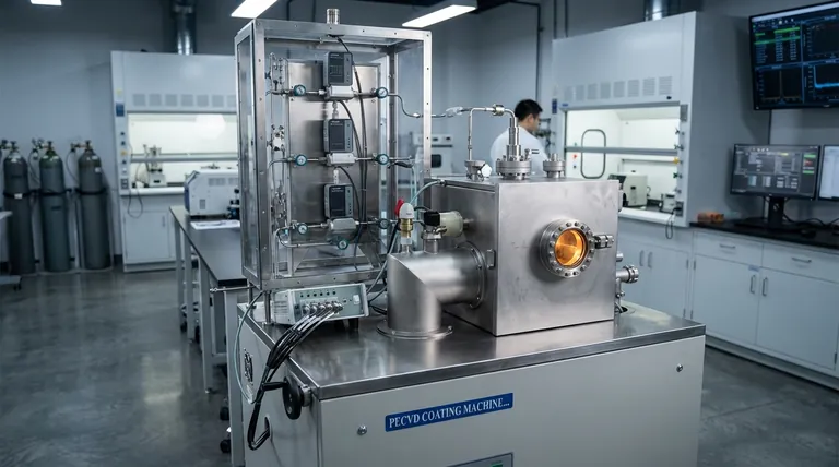
- Chemical Vapor Deposition CVD Equipment System Chamber Slide PECVD Tube Furnace with Liquid Gasifier PECVD Machine
- RF PECVD System Radio Frequency Plasma-Enhanced Chemical Vapor Deposition RF PECVD
- Microwave Plasma Chemical Vapor Deposition MPCVD Machine System Reactor for Lab and Diamond Growth
- Customer Made Versatile CVD Tube Furnace Chemical Vapor Deposition Chamber System Equipment
- 915MHz MPCVD Diamond Machine Microwave Plasma Chemical Vapor Deposition System Reactor
People Also Ask
- What happens during deposition chemistry? Building Thin Films from Gaseous Precursors
- Why is Chemical Vapor Deposition (CVD) equipment uniquely suited for constructing hierarchical superhydrophobic structures?
- What is the chemical vapor deposition growth process? Build Superior Thin Films from the Atom Up
- How expensive is chemical vapor deposition? Understanding the True Cost of High-Performance Coating
- What are the core advantages of PE-CVD in OLED encapsulation? Protect Sensitive Layers with Low-Temp Film Deposition


