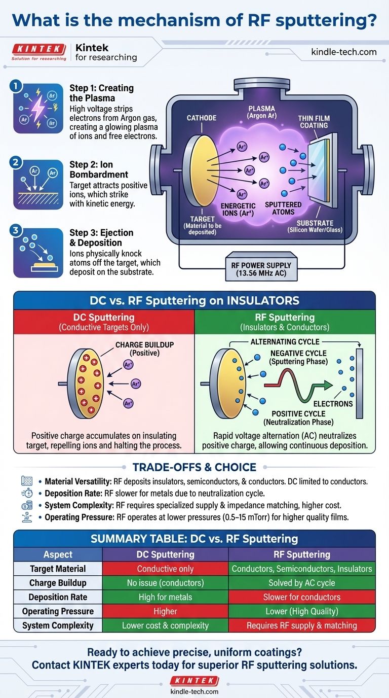
At its core, RF sputtering is a thin-film deposition technique that uses a radio frequency (RF) alternating electric field to create a plasma. This plasma generates energetic ions that collide with a target material, physically knocking atoms off its surface. These ejected atoms then travel through a vacuum and deposit onto a substrate, forming a precise, uniform coating. Its critical advantage is the ability to deposit insulating (non-conductive) materials, which is impossible with simpler DC sputtering methods.
The central challenge in sputtering insulating materials is the buildup of positive charge on the target's surface, which repels the very ions needed to continue the process. RF sputtering solves this by rapidly alternating the voltage, using a brief positive cycle to attract electrons and neutralize this charge, effectively "resetting" the surface for continuous deposition.
The Fundamental Sputtering Process
Sputtering, in any form, is a physical vapor deposition (PVD) method that relies on momentum transfer, much like a cue ball breaking a rack of billiard balls. The process takes place inside a vacuum chamber.
Step 1: Creating the Plasma
First, the chamber is evacuated to a high vacuum. A small amount of an inert gas, typically Argon (Ar), is then introduced at a very low pressure.
Applying a high voltage creates an electric field that strips electrons from the Argon atoms, creating a glowing, ionized gas known as a plasma. This plasma consists of positive argon ions (Ar+) and free electrons.
Step 2: Ion Bombardment
The material to be deposited, known as the target, acts as the cathode. It is given a negative electrical potential, causing it to strongly attract the positively charged Argon ions from the plasma.
These ions accelerate toward the target, striking its surface with significant kinetic energy.
Step 3: Ejection and Deposition
The high-energy impact of an Argon ion physically knocks out, or "sputters," atoms from the target material.
These sputtered atoms travel through the low-pressure chamber and land on the substrate (such as a silicon wafer or piece of glass), gradually building up a thin film.
Why RF is Essential for Insulating Materials
The mechanism described above works perfectly for conductive targets, but it fails completely for insulators like oxides or nitrides when using a simple Direct Current (DC) power source.
The Charge Buildup Problem
In DC sputtering, the target is held at a constant negative voltage. When positive Argon ions strike a conductive target, the excess positive charge is immediately neutralized by the target's abundant free electrons.
However, if the target is an insulator, it has no free electrons. Positive ions striking the surface accumulate, building up a layer of positive charge.
How Positive Charge Halts the Process
This accumulated positive charge on the target's surface begins to repel the incoming positive Argon ions from the plasma.
Eventually, the repulsive force becomes so strong that it prevents any more ions from reaching the target, and the sputtering process grinds to a halt.
The RF Solution: The Alternating Cycle
RF sputtering overcomes this by using an Alternating Current (AC) power source, typically at a fixed radio frequency of 13.56 MHz. This rapidly flips the target's voltage from negative to positive millions of times per second.
The Negative Cycle (The Sputtering Phase)
During the larger, negative portion of the AC cycle, the target behaves just like a DC target. It attracts positive Argon ions, and sputtering occurs as expected. Positive charge begins to build up on the surface.
The Positive Cycle (The Neutralization Phase)
During the brief, positive portion of the cycle, the situation reverses. The target now attracts the highly mobile, negatively charged electrons from the plasma.
These electrons flood the target's surface, completely neutralizing the positive charge that accumulated during the negative cycle. This action "cleans the slate," allowing the next negative cycle to be fully effective. Because electrons are much lighter and more mobile than ions, this neutralization step is extremely fast and efficient.
Understanding the Trade-offs
Choosing RF sputtering involves considering its distinct advantages and disadvantages compared to DC sputtering.
Material Versatility
RF sputtering is the clear winner here. It can deposit virtually any material, including dielectrics (insulators), semiconductors, and conductors. DC sputtering is effectively limited to conductive materials.
Deposition Rate
For depositing conductive metals, RF sputtering is generally slower than DC sputtering. The brief positive cycle is dedicated to charge neutralization, not deposition, which slightly reduces overall efficiency.
System Complexity and Cost
RF systems are more complex and expensive. They require a specialized RF power supply and an impedance matching network to efficiently transfer power to the plasma, adding to the initial cost and operational complexity.
Operating Pressure
RF fields are more efficient at sustaining a plasma. This allows RF sputtering to operate at lower chamber pressures (e.g., 0.5 to 15 mTorr) than DC sputtering. Lower pressure reduces the chance of sputtered atoms colliding with gas molecules, leading to a more direct path to the substrate and potentially higher-quality films.
Making the Right Choice for Your Application
Selecting the correct sputtering method is entirely dependent on your target material and performance requirements.
- If your primary focus is depositing conductive metals at high speed and low cost: DC sputtering is the superior and more economical choice.
- If your primary focus is depositing insulating or dielectric materials (like oxides or nitrides): RF sputtering is the essential and required technology.
- If your primary focus is creating complex alloy films or high-purity coatings: The lower operating pressure of RF sputtering can provide a distinct advantage in film quality, regardless of the material's conductivity.
Ultimately, the choice hinges on the electrical properties of your target material, making RF sputtering the indispensable tool for fabricating the advanced dielectric layers in modern electronics and optical coatings.
Summary Table:
| Aspect | DC Sputtering | RF Sputtering |
|---|---|---|
| Target Material | Conductive materials only | Conductors, semiconductors, and insulators (e.g., oxides, nitrides) |
| Charge Buildup | Not an issue for conductors | Solved by AC cycle neutralization |
| Deposition Rate | High for metals | Slower for conductors |
| Operating Pressure | Higher | Lower (0.5-15 mTorr) |
| System Complexity | Lower cost and complexity | Requires RF power supply and impedance matching |
Ready to achieve precise, uniform coatings on any material?
Whether you're developing advanced electronics, optical coatings, or complex alloy films, KINTEK's RF sputtering equipment is engineered for superior performance and reliability. Our expertise in lab equipment ensures you get the right solution for depositing insulating, semiconducting, and conductive materials with high purity and quality.
Contact our experts today to discuss how our sputtering systems can accelerate your research and production.
Visual Guide
Related Products
- RF PECVD System Radio Frequency Plasma-Enhanced Chemical Vapor Deposition RF PECVD
- Spark Plasma Sintering Furnace SPS Furnace
- Horizontal High Temperature Graphite Vacuum Graphitization Furnace
People Also Ask
- What is the role of RF-PECVD in VFG preparation? Mastering Vertical Growth and Surface Functionality
- How does Radio Frequency Enhanced Plasma Chemical Vapour Deposition (RF-PECVD) work? Learn the Core Principles
- What is plasma enhanced chemical vapour deposition PECVD used for? Enable Low-Temp Thin Films for Electronics & Solar
- What is an example of PECVD? RF-PECVD for High-Quality Thin Film Deposition
- Why is a Matching Network Indispensable in RF-PECVD for Siloxane Films? Ensure Stable Plasma and Uniform Deposition


