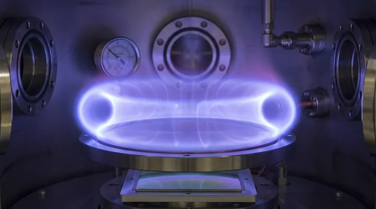
At its core, magnetron sputtering is a physical vapor deposition (PVD) process that uses a combination of an electric and magnetic field to create a plasma. This plasma bombards a source material, known as a target, with high-energy ions. The force of these collisions physically ejects or "sputters" atoms from the target, which then travel through a vacuum and deposit onto a substrate, forming a highly uniform thin film.
The essential role of the magnetron is not to guide the sputtered atoms, but to trap electrons near the target's surface. This magnetic confinement dramatically increases the efficiency of the plasma, leading to a higher rate of ion bombardment and a more controlled, rapid deposition process.
The Fundamental Steps of Magnetron Sputtering
To understand the mechanism, it's best to break it down into a sequence of events, each building upon the last. The entire process takes place within a sealed vacuum chamber.
1. Establishing the Environment
The process begins by placing the target material and the substrate to be coated into a vacuum chamber. The chamber is pumped down to a very low pressure to remove contaminants like oxygen and water vapor.
After reaching a high vacuum, an inert gas, most commonly Argon (Ar), is introduced into the chamber at a controlled low pressure.
2. Creating the Plasma
A high negative voltage, typically several hundred volts (-300V or more), is applied to the target, which acts as the cathode. This creates a strong electric field between the target and the chamber walls (which are often the anode).
This electric field pulls free electrons from the target. These electrons collide with the neutral Argon atoms, knocking an electron off the Argon and creating a positively charged Argon ion (Ar+) and another free electron. This process, called ionization, ignites and sustains the plasma—a cloud of ions, electrons, and neutral gas atoms.
3. The Role of the Magnetic Field
This is the key to magnetron sputtering. A set of permanent magnets is placed behind the target. This creates a magnetic field that is parallel to the target surface.
This magnetic field traps the highly mobile electrons in a path close to the target surface. Instead of escaping to the anode, the electrons are forced into a looping, spiral path.
This trapping dramatically increases the path length of the electrons, which in turn significantly increases the probability that they will collide with and ionize more Argon atoms. This creates a very dense, concentrated plasma directly in front of the target.
4. Ion Bombardment
The newly created, positively charged Argon ions (Ar+) are unaffected by the magnetic field but are strongly attracted to the negatively charged target.
They accelerate across the plasma sheath and crash into the target surface with immense kinetic energy.
5. The Sputtering Event
When a high-energy ion strikes the target, it transfers its momentum to the atoms in the target's lattice structure. This initiates a collision cascade beneath the surface.
If the energy transferred to a surface atom is greater than the energy binding it to the target, that atom is ejected or "sputtered" from the surface. The ejected particles are neutral atoms of the target material.
6. Deposition
These neutral sputtered atoms are not influenced by the electric or magnetic fields. They travel in straight-line paths through the low-pressure environment.
When these atoms reach the substrate, they condense on its surface. Over time, these atoms build up, nucleate, and grow into a continuous, solid thin film of the target material.
Understanding the Key Control Parameters
The efficiency and quality of the film depend on a careful balance of several factors. Understanding these allows for precise control over the final product.
Target Voltage and Power
Increasing the voltage applied to the target increases the kinetic energy of the bombarding ions. Higher energy generally leads to a higher sputter yield (more atoms ejected per ion), but excessive energy can also lead to ion implantation or damage to the substrate.
Magnetic Field Strength
A stronger magnetic field provides better electron confinement. This creates a denser plasma, which increases the ion current and therefore the sputtering rate. The specific design of the magnetic array also determines the erosion pattern, or "racetrack," on the target surface.
Gas Pressure
There is an optimal pressure range for sputtering. If the pressure is too high, the sputtered atoms will collide with too many gas atoms on their way to the substrate, scattering them and reducing both the deposition rate and the film quality. If the pressure is too low, it becomes difficult to sustain a stable plasma.
Making the Right Choice for Your Goal
The settings you choose directly impact the characteristics of your final film. Your primary objective will dictate your process parameters.
- If your primary focus is a high deposition rate: Use a strong magnetic field and sufficient power to maximize plasma density, while carefully tuning gas pressure to avoid excessive scattering.
- If your primary focus is film purity and density: Operate at the lowest possible Argon pressure that can sustain a stable plasma. This increases the mean free path, ensuring sputtered atoms arrive at the substrate with higher energy and minimal gas collisions.
- If your primary focus is coating delicate substrates: Use lower target voltages or employ pulsed DC/RF power supplies. This helps manage the thermal load and energy delivered to the substrate, preventing damage.
By understanding these core mechanisms, you can move from simply running a deposition process to precisely engineering the properties of your thin film.
Summary Table:
| Key Component | Role in the Process |
|---|---|
| Vacuum Chamber | Creates a contaminant-free environment for the process. |
| Inert Gas (Argon) | Ionized to create the plasma that bombards the target. |
| Target (Cathode) | The source material that is bombarded, causing atoms to be ejected. |
| Magnetic Field | Traps electrons near the target, increasing ionization and plasma density. |
| Substrate | The surface where the ejected target atoms deposit to form a thin film. |
Ready to engineer superior thin films with precision?
The mechanism of magnetron sputtering is key to achieving high-quality, uniform coatings for your R&D or production needs. At KINTEK, we specialize in providing advanced lab equipment and consumables tailored to your specific laboratory challenges.
We help you:
- Increase Deposition Rates: Optimize your process for maximum efficiency.
- Improve Film Quality: Achieve the purity and density your applications demand.
- Protect Delicate Substrates: Utilize techniques to coat sensitive materials without damage.
Let our expertise in sputtering technology drive your innovations forward. Contact our team today to discuss your project requirements and discover the right KINTEK solution for you!
Visual Guide

Related Products
- Spark Plasma Sintering Furnace SPS Furnace
- RF PECVD System Radio Frequency Plasma-Enhanced Chemical Vapor Deposition RF PECVD
People Also Ask
- What is the process fundamentals of spark plasma sintering? Achieve Rapid, High-Density Material Consolidation
- What are the fundamentals of spark plasma sintering process? Unlock Rapid, High-Performance Material Consolidation
- Why are Spark Plasma Sintering (SPS) furnaces or hot presses utilized in the preparation of Li3PS4 solid electrolytes?
- What is the difference between spark plasma sintering and flash sintering? A Guide to Advanced Sintering Methods
- What is the mechanism of SPS process? A Deep Dive into Rapid, Low-Temperature Sintering

