In technical terms, a method of deposition is any process that applies a thin film of a source material onto a surface, known as a substrate. This is typically achieved by converting the source material into a gaseous form—through processes like evaporation or sputtering—within a vacuum, which then condenses and solidifies on the substrate to form the desired coating.
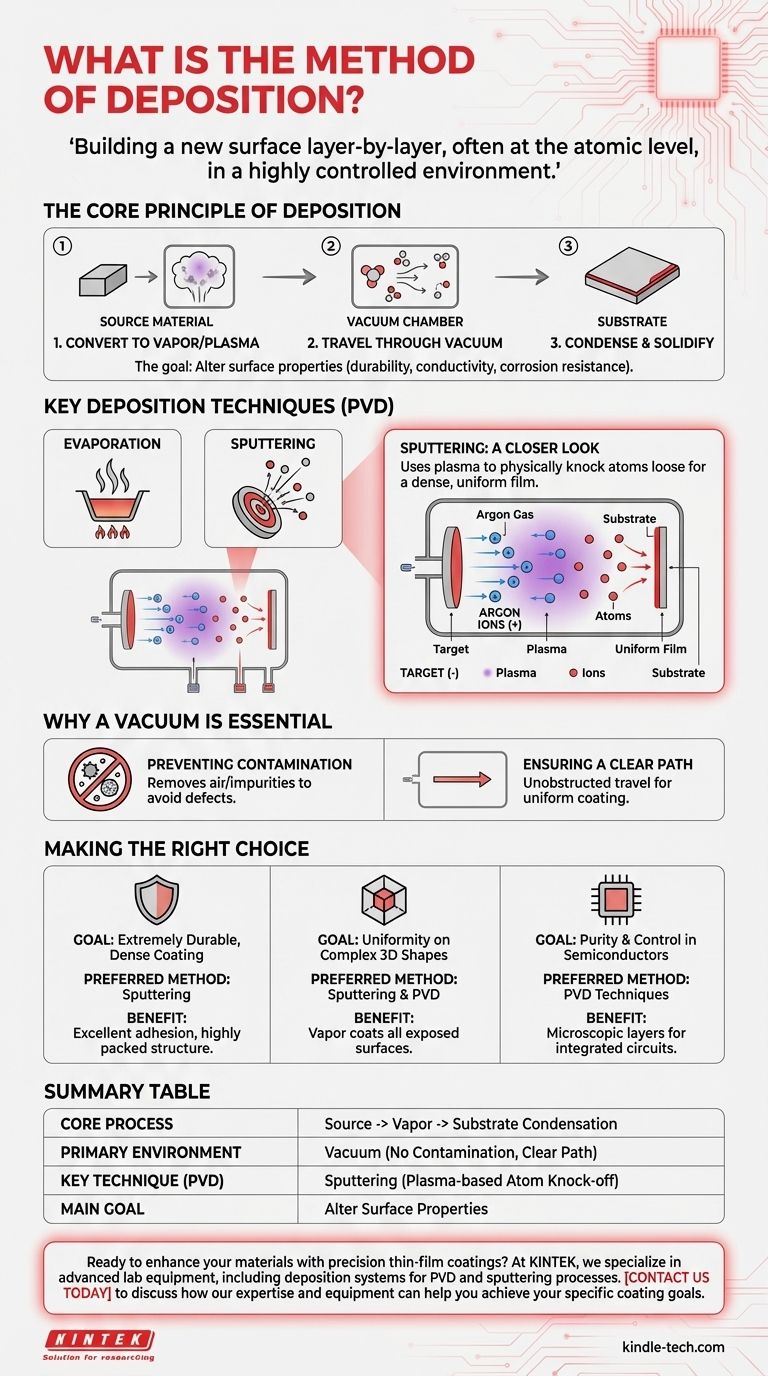
The core concept behind deposition is not about applying a liquid coating like paint, but about building a new surface layer-by-layer, often at the atomic level, by transferring material from a source to a target within a highly controlled environment.
The Core Principle of Deposition
What Happens During Deposition?
At its heart, every deposition process involves three fundamental steps. First, a source material is converted into a vapor or plasma. Second, this gaseous material travels through a controlled environment, usually a vacuum chamber. Finally, it condenses onto a substrate to form a solid, thin film.
The Role of the Source Material
The source material is the substance you want to form the coating. It can be a metal, ceramic, or other compound. The specific deposition technique is often chosen based on the properties of this material, such as its melting point.
The Importance of the Substrate
The substrate is simply the object being coated. The goal of deposition is to alter the surface properties of the substrate—for example, to make it more durable, electrically conductive, or resistant to corrosion.
Key Deposition Techniques
Physical Vapor Deposition (PVD)
Physical Vapor Deposition (PVD) is not a single method but a family of processes. As the name implies, they use physical means—like heating or bombardment—to convert the source material into a vapor. The references highlight two primary PVD methods: evaporation and sputtering.
Sputtering: A Closer Look
Sputtering is a sophisticated PVD technique that doesn't rely on melting the source material. Instead, a chemically inert gas, such as argon, is introduced into the vacuum chamber and energized to create a plasma.
Positively charged ions from this plasma are accelerated into the negatively charged source material (the "target"). This high-energy collision physically knocks atoms loose from the source, which then travel and deposit onto the substrate, forming a very uniform and dense film.
Why a Vacuum is Essential
Preventing Contamination
The primary reason for performing deposition in a vacuum is to remove air and other unwanted particles. If these particles were present, they would collide with the vaporized source material, react with it, and contaminate the final film, leading to defects and poor quality.
Ensuring a Clear Path
A vacuum also provides an unobstructed path for the vaporized atoms or molecules to travel from the source to the substrate. This ensures an efficient and direct deposition process, which is critical for creating high-quality, uniform coatings.
Making the Right Choice for Your Goal
The specific deposition method used is determined by the desired properties of the final coating and the material being deposited.
- If your primary focus is creating an extremely durable, dense coating: Sputtering is often preferred because the high energy of the process results in excellent adhesion and a highly packed film structure.
- If your primary focus is coating a complex, 3D shape uniformly: Sputtering and other PVD methods are highly effective as the vapor can coat all exposed surfaces within the chamber.
- If your primary focus is purity and control in semiconductor manufacturing: PVD techniques are fundamental for laying down the microscopic layers of conductive and insulating materials that form integrated circuits.
Ultimately, deposition methods give us precise control over a material's surface, enabling the creation of advanced products and technologies.
Summary Table:
| Aspect | Key Detail |
|---|---|
| Core Process | Converting a source material into a vapor that condenses on a substrate. |
| Primary Environment | Vacuum chamber to prevent contamination and ensure a clear path. |
| Key Technique (PVD) | Sputtering: Uses plasma to knock atoms from a target for a dense, uniform film. |
| Main Goal | To alter surface properties like durability, conductivity, or corrosion resistance. |
Ready to enhance your materials with precision thin-film coatings?
At KINTEK, we specialize in advanced lab equipment, including deposition systems for PVD and sputtering processes. Whether you're in semiconductor manufacturing, R&D, or producing durable components, our solutions deliver the high-quality, uniform coatings you need.
Contact us today to discuss how our expertise and equipment can help you achieve your specific coating goals.
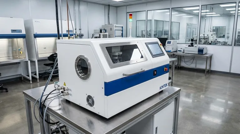
Visual Guide
Related Products
- Chemical Vapor Deposition CVD Equipment System Chamber Slide PECVD Tube Furnace with Liquid Gasifier PECVD Machine
- Vacuum Induction Melting Spinning System Arc Melting Furnace
- Spark Plasma Sintering Furnace SPS Furnace
- Split Chamber CVD Tube Furnace with Vacuum Station Chemical Vapor Deposition System Equipment Machine
- Multi Heating Zones CVD Tube Furnace Machine Chemical Vapor Deposition Chamber System Equipment
People Also Ask
- What happens during deposition chemistry? Building Thin Films from Gaseous Precursors
- What is plasma enhanced chemical vapor deposition PECVD equipment? A Guide to Low-Temperature Thin Film Deposition
- Why is Chemical Vapor Deposition (CVD) equipment uniquely suited for constructing hierarchical superhydrophobic structures?
- What is the chemical vapor deposition growth process? Build Superior Thin Films from the Atom Up
- What are the core advantages of PE-CVD in OLED encapsulation? Protect Sensitive Layers with Low-Temp Film Deposition


