In essence, Plasma-Enhanced Chemical Vapor Deposition (PECVD) is a process used to deposit thin films onto a substrate from a gas state. Unlike traditional Chemical Vapor Deposition (CVD), which relies on high temperatures to drive chemical reactions, PECVD uses the energy from a plasma to initiate these reactions at a much lower temperature. This allows for the coating of a wider range of materials, including those sensitive to heat.
The core advantage of PECVD is its ability to use plasma energy instead of high thermal energy. This fundamental difference unlocks the ability to create high-quality, functional thin films on temperature-sensitive materials that would be damaged by other methods.
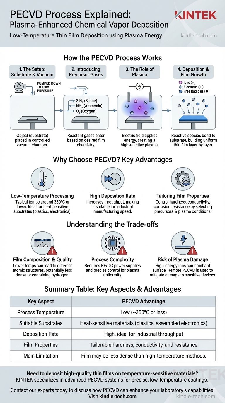
How the PECVD Process Works
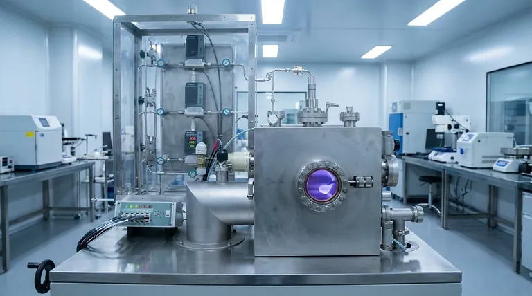
To understand PECVD, it's best to break it down into its constituent steps. The entire process takes place within a controlled vacuum chamber to ensure purity and process stability.
The Setup: Substrate and Vacuum
First, the object to be coated, known as the substrate, is placed inside the reaction chamber. The chamber is then pumped down to a low pressure, creating a vacuum that removes contaminants.
Introducing Precursor Gases
Reactant gases, also known as precursors, are then introduced into the chamber. The specific gas chemistry is chosen based on the desired properties of the final film. For example, gases containing silicon are used to create silicon dioxide or silicon nitride films.
The Role of Plasma
This is the defining step of PECVD. An electric field is applied across electrodes within the chamber, igniting the precursor gases and turning them into a plasma, often seen as a characteristic glow discharge.
This plasma is a high-energy state of matter where gas molecules are fragmented into a mix of ions, electrons, and highly reactive free radicals. This energy is what drives the necessary chemical reactions, replacing the need for extreme heat.
Deposition and Film Growth
The reactive chemical species created in the plasma then diffuse toward the substrate. Upon reaching the cooler surface of the substrate, they react and bond, depositing a solid, thin film. This process builds up layer by layer, forming a uniform coating with carefully controlled thickness and properties.
Why Choose PECVD?
PECVD is not just one of several options; it solves specific engineering challenges that other methods cannot easily address.
The Low-Temperature Advantage
The most significant benefit is the low processing temperature, typically around 350°C or even lower. Traditional CVD can require temperatures exceeding 600-800°C. This makes PECVD ideal for coating plastics, assembled electronic devices, and other substrates that cannot withstand high heat.
High Deposition Rate
Compared to some other low-temperature techniques like Low-Pressure CVD (LPCVD), PECVD often has a higher deposition rate. This increases throughput, making it highly valuable for industrial manufacturing where speed is a critical factor.
Tailoring Film Properties
The properties of the final film are directly linked to the precursor gases and plasma conditions. By carefully selecting the precursors, engineers can tailor the film's characteristics, such as its hardness, electrical conductivity, corrosion resistance, or optical properties, for a specific application.
Understanding the Trade-offs
No process is perfect. Being a trusted advisor means acknowledging the limitations and potential downsides of a technology.
Film Composition and Quality
Because PECVD operates at lower temperatures, the resulting films can have a different atomic structure than those from high-temperature processes. They may be less dense or contain incorporated elements from the precursor gas, such as hydrogen. This isn't necessarily a flaw but is a critical design consideration.
Process Complexity
The use of RF or DC power supplies to generate and sustain the plasma adds a layer of complexity to the equipment and process control. Managing plasma uniformity is crucial for achieving a consistent coating across the entire substrate.
The Risk of Plasma Damage
In some configurations, the high-energy ions within the plasma can physically bombard the substrate surface. While this can sometimes be beneficial for film adhesion, it can also cause damage to sensitive electronic devices. Advanced techniques like Remote PECVD, where the plasma is generated away from the substrate, were developed to mitigate this risk.
Making the Right Choice for Your Goal
Selecting a deposition method depends entirely on the constraints and desired outcome of your project.
- If your primary focus is coating heat-sensitive substrates: PECVD is often the default and superior choice due to its fundamentally lower processing temperature.
- If your primary focus is achieving the highest possible film purity and density: You may need to evaluate high-temperature methods like LPCVD, but you must weigh this against your substrate's thermal limits.
- If your primary focus is rapid production throughput for robust materials: PECVD's high deposition rate makes it a very strong candidate for industrial-scale applications.
By understanding its core mechanism and trade-offs, you can effectively leverage PECVD to engineer material surfaces for a specific function.
Summary Table:
| Key Aspect | PECVD Advantage |
|---|---|
| Process Temperature | Low (~350°C or less) |
| Suitable Substrates | Heat-sensitive materials (plastics, assembled electronics) |
| Deposition Rate | High, ideal for industrial throughput |
| Film Properties | Tailorable hardness, conductivity, and resistance |
| Main Limitation | Film may be less dense than high-temperature methods |
Need to deposit high-quality thin films on temperature-sensitive materials? KINTEK specializes in advanced lab equipment, including PECVD systems, to help you achieve precise, low-temperature coatings for your research or production needs. Our expertise ensures you get the right solution for coating plastics, electronics, and other delicate substrates. Contact our experts today to discuss how PECVD can enhance your laboratory's capabilities!
Visual Guide
Related Products
- Chemical Vapor Deposition CVD Equipment System Chamber Slide PECVD Tube Furnace with Liquid Gasifier PECVD Machine
- RF PECVD System Radio Frequency Plasma-Enhanced Chemical Vapor Deposition RF PECVD
- Inclined Rotary Plasma Enhanced Chemical Vapor Deposition PECVD Equipment Tube Furnace Machine
- Inclined Rotary Plasma Enhanced Chemical Vapor Deposition PECVD Equipment Tube Furnace Machine
- 915MHz MPCVD Diamond Machine Microwave Plasma Chemical Vapor Deposition System Reactor
People Also Ask
- Why is Chemical Vapor Deposition (CVD) equipment uniquely suited for constructing hierarchical superhydrophobic structures?
- What happens during deposition chemistry? Building Thin Films from Gaseous Precursors
- What is the chemical vapor deposition growth process? Build Superior Thin Films from the Atom Up
- What are the advantages of chemical vapor deposition? Achieve Superior Thin Films for Your Lab
- How expensive is chemical vapor deposition? Understanding the True Cost of High-Performance Coating


