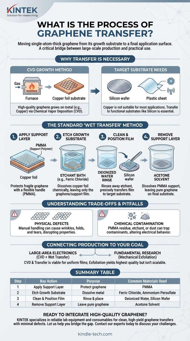
To put it simply, graphene transfer is the critical process of moving a single-atom-thick layer of graphene from the substrate it was grown on to a different, final substrate where it can be used. This multi-step procedure typically involves coating the graphene with a supportive polymer, dissolving the original growth substrate, and carefully placing the remaining polymer/graphene film onto a target surface before removing the support layer.
The core challenge in using graphene is not just its production, but the delicate transfer process that bridges the gap between large-scale growth and practical application. The quality of this transfer directly dictates the final performance of the graphene film.
Why is a Transfer Process Necessary?
To understand the need for transfer, we must first look at how high-quality graphene is made. The most common method for producing large, uniform sheets of graphene is Chemical Vapor Deposition (CVD).
The CVD Growth Method
CVD involves heating a substrate, typically a metal foil like copper or nickel, in a furnace. A carbon-containing gas (like methane) is then introduced, which breaks down at high temperatures. The carbon atoms then rearrange themselves on the surface of the metal foil, forming a continuous, single layer of graphene.
The Substrate Dilemma
The copper foil used for CVD growth is excellent for catalyzing graphene formation but is not useful for most final applications, such as electronics or sensors. To use the graphene, you must get it off the copper and onto a functional substrate, such as a silicon wafer or a flexible plastic sheet. This is where the transfer process becomes essential.
The Standard "Wet Transfer" Method Explained
The most common and illustrative technique is known as wet transfer, which uses liquids to etch and clean the graphene film.
Step 1: Apply a Support Layer
First, a supportive polymer layer, most commonly PMMA (the same plastic used in Plexiglas), is coated directly on top of the graphene/copper foil. This polymer acts as a flexible, transparent handle, preventing the fragile, one-atom-thick graphene sheet from tearing or folding during handling.
Step 2: Etch the Growth Substrate
The entire PMMA/graphene/copper sandwich is then placed in a chemical bath, or "etchant" (like ferric chloride or ammonium persulfate). This chemical specifically dissolves the copper foil without damaging the graphene or the PMMA support layer. After several hours, only the transparent PMMA/graphene film is left floating in the liquid.
Step 3: Clean and Position the Film
The delicate film is carefully moved to a bath of deionized water to rinse away any residual etchant chemicals. It is then "fished" out of the water using the target substrate (e.g., a silicon wafer). This step is extremely precise work, as wrinkles or bubbles can easily form.
Step 4: Remove the Support Layer
After the film is positioned on the target substrate and dried, the final step is to remove the PMMA support layer. This is done by submerging the entire sample in a solvent, such as acetone, which dissolves the PMMA and leaves only the pure graphene sheet on the final substrate.
Understanding the Trade-offs and Pitfalls
While necessary, the transfer process is the most significant source of defects and contamination in CVD graphene, directly impacting its final quality.
The Risk of Physical Defects
The manual handling involved in moving and placing the film can easily introduce wrinkles, folds, and microscopic tears. These structural imperfections disrupt the graphene's perfect hexagonal lattice, severely degrading its exceptional electronic and mechanical properties.
The Problem of Chemical Contamination
Residue from the PMMA support layer, the etchant, or even ambient dust can get trapped between the graphene and the new substrate. This contamination can alter graphene's electrical behavior, making it less reliable for high-performance electronics.
The Bottleneck for Manufacturing
While CVD allows for the production of large sheets of graphene, the transfer process is often slow, delicate, and difficult to automate. This creates a significant bottleneck for scaling up graphene production for widespread commercial use.
Connecting Production to Your Goal
Your choice of graphene production and handling depends entirely on your end goal.
- If your primary focus is large-area electronics or transparent conductors: CVD growth followed by a meticulous wet transfer is the most viable path to obtaining high-quality, uniform films on functional wafers.
- If your primary focus is fundamental research or initial material testing: Mechanical exfoliation (the "Scotch tape method") produces the highest quality graphene flakes and bypasses the transfer process entirely, but it is not scalable and yields only tiny, irregularly shaped samples.
Understanding that graphene's journey involves both growth and transfer is the key to harnessing its true technological potential.
Summary Table:
| Step | Key Action | Purpose | Common Materials Used |
|---|---|---|---|
| 1 | Apply Support Layer | Protect graphene during handling | PMMA (Polymer) |
| 2 | Etch Growth Substrate | Dissolve original metal foil | Ferric Chloride, Ammonium Persulfate |
| 3 | Clean & Position Film | Rinse and place on target substrate | Deionized Water, Silicon Wafer |
| 4 | Remove Support Layer | Leave pure graphene on final substrate | Acetone Solvent |
Ready to integrate high-quality graphene into your research or product development?
The graphene transfer process is delicate, but having the right lab equipment is crucial for success. KINTEK specializes in providing the reliable lab equipment and consumables—from precise etching baths to cleanroom materials—that your laboratory needs to achieve clean, high-yield graphene transfers with minimal defects and contamination.
Let us help you bridge the gap between graphene production and practical application. Contact our experts today to discuss how our solutions can support your specific graphene handling and transfer challenges.
Visual Guide
Related Products
- HFCVD Machine System Equipment for Drawing Die Nano-Diamond Coating
- Chemical Vapor Deposition CVD Equipment System Chamber Slide PECVD Tube Furnace with Liquid Gasifier PECVD Machine
- Customer Made Versatile CVD Tube Furnace Chemical Vapor Deposition Chamber System Equipment
- RF PECVD System Radio Frequency Plasma-Enhanced Chemical Vapor Deposition RF PECVD
- 915MHz MPCVD Diamond Machine Microwave Plasma Chemical Vapor Deposition System Reactor
People Also Ask
- What is the function of tungsten filaments in HFCVD? Powering Diamond Film Synthesis with Thermal Excitation
- What types of substrates are used in CVD to facilitate graphene films? Optimize Graphene Growth with the Right Catalyst
- What is the specific function of the metal filament in HF-CVD? Key Roles in Diamond Growth
- What are the disadvantages and challenges of the HFCVD method? Overcome Growth Limits and Filament Issues
- What is the full form of HFCVD? A Guide to Hot Filament Chemical Vapor Deposition