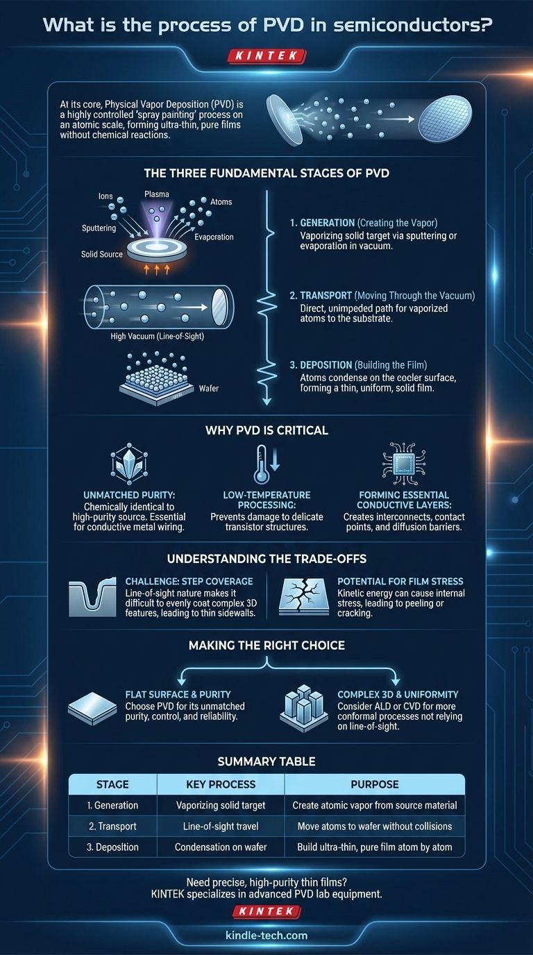
At its core, Physical Vapor Deposition (PVD) is a highly controlled "spray painting" process on an atomic scale. It involves vaporizing a solid source material inside a high-vacuum chamber and allowing the vapor to travel and condense onto a semiconductor wafer. This method forms an ultra-thin, pure film one atom at a time, and is defined by the fact that no chemical reactions are used to create the final layer.
The central principle of PVD is the physical transport of material from a source to a substrate without any chemical alteration. This makes it an indispensable tool for depositing the pure metal layers that form the wiring and connection points in modern microchips.
The Three Fundamental Stages of PVD
The entire PVD process, regardless of the specific technique used, can be broken down into three distinct and sequential stages. Understanding this flow is key to understanding the process's capabilities and limitations.
Stage 1: Generation (Creating the Vapor)
The first step is to convert a solid source material, known as the target, into a gaseous or vapor phase. This must be done with precision inside the vacuum chamber.
The most common methods for this are sputtering, where the target is bombarded with high-energy ions from a plasma, knocking atoms loose, or evaporation, where the target is heated until its atoms boil off into the vacuum.
Stage 2: Transport (Moving Through the Vacuum)
Once liberated from the target, the vaporized atoms travel through the vacuum chamber toward the substrate (the semiconductor wafer).
The high vacuum is critical. It ensures there are very few air or gas molecules for the traveling atoms to collide with, allowing them a direct, unimpeded path. This direct path is often referred to as line-of-sight transport.
Stage 3: Deposition (Building the Film)
When the vaporized atoms reach the cooler surface of the wafer, they rapidly lose energy and condense back into a solid state.
This condensation builds up layer by layer, atom by atom, to form a thin, uniform, and solid film. The properties of this film—such as its density and purity—are tightly controlled by factors like the vacuum level, temperature, and energy of the incoming atoms.
Why PVD is Critical in Semiconductor Manufacturing
PVD is not just one of many options; it is a foundational process used for specific, critical layers where its unique advantages are non-negotiable.
Unmatched Purity
Because PVD is a physical process, the deposited film is chemically identical to the high-purity source target. There are no chemical precursors or byproducts to introduce impurities. This is essential for creating highly conductive metal wiring.
Low-Temperature Processing
PVD generally operates at lower temperatures than its chemical counterpart, Chemical Vapor Deposition (CVD). This is crucial in modern chip fabrication, as it prevents damage to the complex, delicate transistor structures already built on the wafer in previous steps.
Forming Essential Conductive Layers
PVD is the go-to method for depositing the metal layers that act as the chip's wiring, known as interconnects. It's also used for creating contact points and diffusion barriers, which prevent different materials from mixing and degrading the chip's performance over time.
Understanding the Inherent Trade-offs
No process is perfect, and a trusted advisor must highlight the limitations. The physical nature of PVD creates distinct challenges that engineers must manage.
The Challenge of "Step Coverage"
The biggest limitation of PVD is its line-of-sight nature. Like a spray-paint can, it coats what it can "see." This makes it difficult to evenly coat complex, three-dimensional chip features like deep, narrow trenches.
The top surfaces of these features will receive a thick coating, but the vertical sidewalls and the bottom of the trench will receive a much thinner layer, or none at all. This poor "step coverage" can create defects and open circuits.
Potential for Film Stress
The kinetic energy of atoms striking the wafer surface can create internal stress within the deposited film. If not properly controlled, this stress can cause the film to peel or crack, leading to device failure.
Making the Right Choice for Your Goal
Your choice of deposition technique hinges entirely on the specific layer's function and the topology of the surface you are coating.
- If your primary focus is depositing a pure, highly conductive metal layer on a relatively flat surface: PVD is the industry-standard choice for its unmatched purity, control, and reliability.
- If your primary focus is creating a perfectly uniform coating over a complex 3D structure with deep trenches: You would need a more conformal process like Atomic Layer Deposition (ALD) or Chemical Vapor Deposition (CVD), which do not rely on line-of-sight.
Ultimately, understanding PVD's physical, line-of-sight nature is the key to leveraging its strengths and mitigating its weaknesses in advanced fabrication.
Summary Table:
| Stage | Key Process | Purpose |
|---|---|---|
| 1. Generation | Vaporizing solid target via sputtering or evaporation | Create atomic vapor from source material |
| 2. Transport | Line-of-sight travel in high vacuum | Move vaporized atoms to wafer without collisions |
| 3. Deposition | Condensation on wafer surface | Build ultra-thin, pure film atom by atom |
Need precise, high-purity thin films for your semiconductor fabrication? KINTEK specializes in advanced PVD lab equipment and consumables, delivering the reliability and control essential for modern microchip manufacturing. Contact our experts today to discuss how our solutions can enhance your deposition process and improve chip performance.
Visual Guide
Related Products
- RF PECVD System Radio Frequency Plasma-Enhanced Chemical Vapor Deposition RF PECVD
- Inclined Rotary Plasma Enhanced Chemical Vapor Deposition PECVD Equipment Tube Furnace Machine
- Vacuum Hot Press Furnace Machine for Lamination and Heating
- Chemical Vapor Deposition CVD Equipment System Chamber Slide PECVD Tube Furnace with Liquid Gasifier PECVD Machine
- Microwave Plasma Chemical Vapor Deposition MPCVD Machine System Reactor for Lab and Diamond Growth
People Also Ask
- Why does PECVD commonly use RF power input? For Precise Low-Temperature Thin Film Deposition
- What is plasma activated chemical vapour deposition method? A Low-Temperature Solution for Advanced Coatings
- What are the applications of PECVD? Essential for Semiconductors, MEMS, and Solar Cells
- What are the advantages of PECVD? Enable Low-Temperature, High-Quality Thin-Film Deposition
- What is an example of PECVD? RF-PECVD for High-Quality Thin Film Deposition