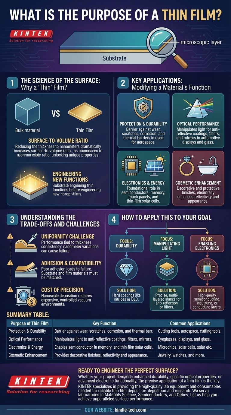
The fundamental purpose of a thin film is to apply a microscopic layer of material onto a surface to fundamentally alter its properties. This allows a base material, or substrate, to gain new functions—such as enhanced durability, specific optical qualities, or electrical conductivity—that it does not possess on its own.
The core value of a thin film isn't just about adding a layer; it's about leveraging the unique physics that emerge at the nanoscale. By reducing a material's thickness to mere atoms, its properties change, allowing us to engineer surfaces for highly specific and powerful applications.
Why a 'Thin' Film? The Science of the Surface
The Power of Surface-to-Volume Ratio
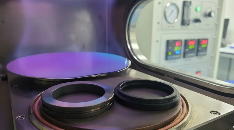
A thin film is a layer of material ranging from a few nanometers to several micrometers thick.
At this scale, the surface-to-volume ratio is dramatically increased compared to the same material in its bulk form.
This change fundamentally alters how the material behaves, unlocking unique mechanical, optical, and electrical properties that are otherwise unobservable.
Engineering New Functions
Applying a thin film is not just about coating a surface; it's about adding a new, engineered function.
The underlying object (the substrate) provides the structure, while the thin film provides a specialized surface performance.
Key Applications: Modifying a Material's Function
For Protection and Durability
One of the most common uses is creating a barrier against the environment.
These films protect surfaces from wear, scratches, and corrosion on everything from cutting tools to optical lenses.
In extreme cases, they act as thermal barriers on components in the aerospace industry, protecting them from intense heat.
For Optical Performance
Thin films are critical for manipulating light.
Multiple layers can be stacked to create anti-reflective coatings on eyeglasses, filters for specific wavelengths of light, or highly reflective mirrors.
This technology is essential in automotive head-up displays and thermally insulated architectural glass.
For Electronics and Energy
The modern electronics industry is built on thin films.
They are fundamental to manufacturing semiconductor devices, memory storage, and touch panels.
They are also used to convert light into power in thin-film solar cells and are being developed for next-generation batteries.
For Cosmetic Enhancement
Thin films can be used purely for aesthetic purposes.
They provide the decorative and protective finishes on items like jewelry and bathroom fittings, often enhancing reflectivity and appearance.
Understanding the Trade-offs and Challenges
The Challenge of Uniformity
The performance of a thin film is directly tied to its thickness and consistency.
Achieving a perfectly uniform layer, especially over complex shapes, is a significant manufacturing challenge where even nanometer-scale variations can cause failure.
Adhesion and Substrate Compatibility
A thin film is only effective if it adheres perfectly to the substrate.
Poor adhesion can lead to delamination, flaking, and complete failure of the film's intended function. The substrate and film materials must be carefully matched.
The Cost of Precision
Depositing materials at the nanoscale requires highly specialized and expensive equipment.
Processes like physical and chemical vapor deposition occur in controlled vacuum environments, adding significant complexity and cost to manufacturing.
How to Apply This to Your Goal
Choosing a thin film strategy depends entirely on the problem you need to solve.
- If your primary focus is durability: You will likely need hard, inert coatings like nitrides (e.g., TiN) or diamond-like carbon (DLC) to resist wear and corrosion.
- If your primary focus is manipulating light: The solution involves precise, multi-layered stacks of dielectric materials to create anti-reflection coatings or optical filters.
- If your primary focus is enabling electronics: You require high-purity layers of semiconducting, insulating, or conducting materials deposited with extreme precision.
Ultimately, thin films are a foundational technology that allows us to engineer the surfaces of materials to achieve nearly any desired outcome.
Summary Table:
| Purpose of Thin Film | Key Function | Common Applications |
|---|---|---|
| Protection & Durability | Creates a barrier against wear, corrosion, and heat. | Cutting tools, aerospace components, optical lenses. |
| Optical Performance | Manipulates light for anti-reflection, filtering, or reflection. | Eyeglasses, architectural glass, displays, mirrors. |
| Electronics & Energy | Enables semiconductor devices, solar cells, and batteries. | Microchips, memory storage, touch panels, thin-film PV. |
| Cosmetic Enhancement | Provides decorative and protective finishes. | Jewelry, watches, bathroom and automotive fittings. |
Ready to engineer the perfect surface for your application?
Whether your project demands enhanced durability, specific optical properties, or advanced electronic functionality, the precise application of a thin film is the key. KINTEK specializes in providing the high-quality lab equipment and consumables needed for reliable thin film deposition and research.
We serve laboratories and researchers focused on:
- Materials Science: Developing protective and functional coatings.
- Semiconductors & Electronics: Fabricating microchips and devices.
- Optics & Photonics: Creating filters, mirrors, and anti-reflective coatings.
Let us help you achieve unparalleled surface performance. Contact our experts today to discuss your specific substrate and thin film requirements!
Visual Guide
Related Products
- Aluminum-Plastic Flexible Packaging Film for Lithium Battery Packaging
- Thin-Layer Spectral Electrolysis Electrochemical Cell
People Also Ask
- What is the difference between single layer film and multi layer film? A Guide to Material Selection
- How to check if a lithium battery is good? Safely Test Voltage, Capacity & Internal Resistance
- What are the properties of Aluminium (Al) relevant to its use in coatings? High Reflectivity & Conductivity Explored
- What are the three types of lamination? Choose the Perfect Finish for Your Print Project
- What is the difference between monolayer and multilayer film? Choose the Right Packaging for Your Product

