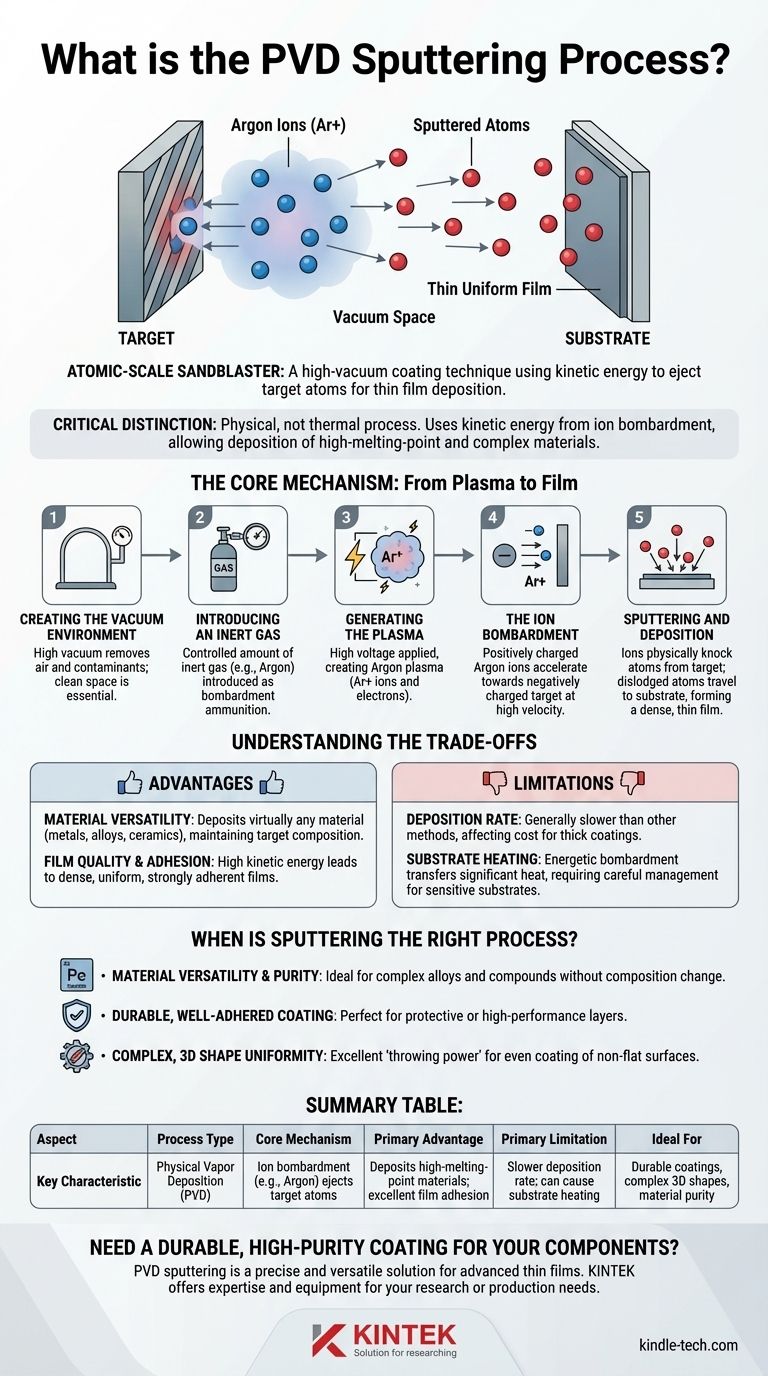
At its core, PVD sputtering is a high-vacuum coating technique that functions like an atomic-scale sandblaster. In this process, a source material, known as the "target," is bombarded by energetic ions from a plasma. This collision physically knocks atoms loose from the target, which then travel through the vacuum and deposit onto a component, called the "substrate," to form an exceptionally thin and uniform film.
The critical distinction of sputtering is that it is a physical, not thermal, process. Instead of melting a material to create a vapor, it uses kinetic energy from ion bombardment to eject atoms, allowing for the deposition of materials with very high melting points or complex compositions.
The Core Mechanism: From Plasma to Film
To truly understand sputtering, it's best to visualize it as a sequence of precise, controlled steps that occur within a vacuum chamber. Each step builds upon the last to construct a new surface, atom by atom.
Step 1: Creating the Vacuum Environment
The entire process happens at very low pressure. This is essential to remove air and other gas contaminants that could react with the coating material or impede the free travel of sputtered atoms. A clean, empty space is the canvas for the process.
Step 2: Introducing an Inert Gas
A small, controlled amount of an inert gas—most commonly Argon (Ar)—is introduced into the chamber. This gas is stable and will not chemically react with the target material. Instead, it will be used as the "ammunition" for the bombardment.
Step 3: Generating the Plasma
A high voltage is applied within the chamber, energizing the argon gas. This electrical field strips electrons from the argon atoms, creating a cloud of positively charged argon ions and free electrons. This ionized gas is known as a plasma.
Step 4: The Ion Bombardment
The target (the block of material to be deposited) is given a strong negative electrical charge. The positively charged argon ions in the plasma are naturally and powerfully accelerated toward this negatively charged target. They collide with its surface at high velocity.
Step 5: Sputtering and Deposition
The impact of each argon ion is energetic enough to physically knock out, or "sputter," atoms from the target material. These dislodged atoms travel in a straight line through the vacuum until they strike the substrate, which is strategically placed to intercept them. Upon hitting the substrate, they condense and build up, layer by layer, to form a dense, thin film.
Understanding the Trade-offs
Sputtering is an incredibly powerful and versatile technique, but it involves specific trade-offs that make it suitable for some applications and less so for others. Understanding these is key to making an informed decision.
The Advantage: Material Versatility
Because sputtering does not rely on melting, it can be used to deposit virtually any material. This includes metals, alloys, ceramics, and other compounds that would be difficult or impossible to evaporate. The composition of the target material is faithfully reproduced in the final film.
The Advantage: Film Quality and Adhesion
The sputtered atoms arrive at the substrate with significant kinetic energy. This energy helps them form a very dense, uniform film with strong adhesion to the substrate surface. The coatings are often more durable than those produced by other methods.
The Limitation: Deposition Rate
Generally, sputtering is a slower process compared to other PVD techniques like thermal evaporation. For applications requiring very thick coatings or extremely high throughput, this slower rate can be a significant factor in cost and production time.
The Limitation: Substrate Heating
The constant bombardment of energetic particles (both sputtered atoms and plasma ions) can transfer a significant amount of heat to the substrate. For heat-sensitive substrates, such as certain plastics or biological components, this heating effect must be carefully managed or mitigated.
When is Sputtering the Right Process?
Choosing a deposition method depends entirely on the desired outcome for your film and substrate. Sputtering's unique characteristics make it the superior choice for specific goals.
- If your primary focus is material versatility and purity: Sputtering is ideal because it can deposit a vast range of materials, including complex alloys and compounds, without altering their composition.
- If your primary focus is a durable, well-adhered coating: The energetic nature of the sputtering process results in dense films with excellent adhesion, making it perfect for protective or high-performance layers.
- If your primary focus is coating a complex, 3D shape uniformly: Sputtering provides excellent "throwing power," meaning it can coat non-flat surfaces more evenly than line-of-sight deposition methods.
Ultimately, PVD sputtering is a cornerstone of modern materials science, enabling the precise construction of advanced films for everything from microelectronics to medical implants.
Summary Table:
| Aspect | Key Characteristic |
|---|---|
| Process Type | Physical Vapor Deposition (PVD) |
| Core Mechanism | Ion bombardment (e.g., Argon) ejects target atoms |
| Primary Advantage | Deposits high-melting-point materials; excellent film adhesion |
| Primary Limitation | Slower deposition rate; can cause substrate heating |
| Ideal For | Durable coatings, complex 3D shapes, material purity |
Need a Durable, High-Purity Coating for Your Components?
PVD sputtering is a precise and versatile solution for creating advanced thin films. If your project requires exceptional material versatility, strong film adhesion, or uniform coating on complex shapes, KINTEK has the expertise and equipment to help.
We specialize in providing lab equipment and consumables for cutting-edge deposition processes. Contact our experts today to discuss how our solutions can enhance your research or production outcomes.
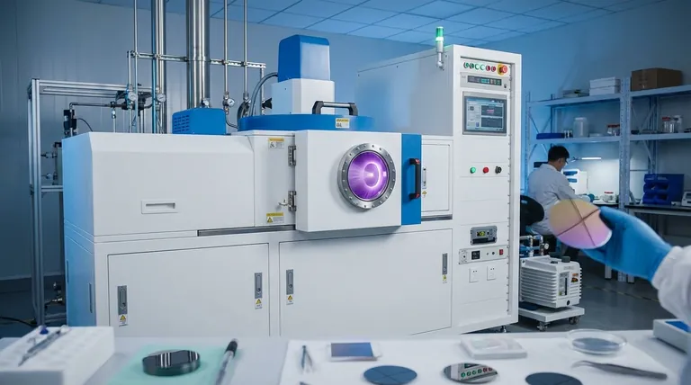
Visual Guide
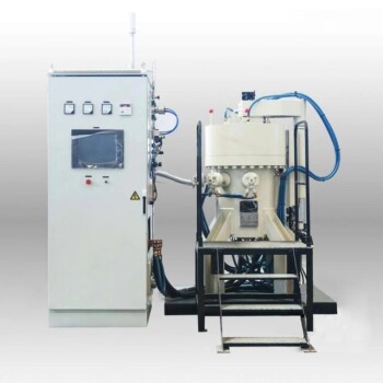
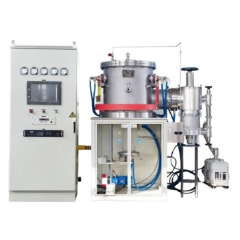
Related Products
- RF PECVD System Radio Frequency Plasma-Enhanced Chemical Vapor Deposition RF PECVD
- Chemical Vapor Deposition CVD Equipment System Chamber Slide PECVD Tube Furnace with Liquid Gasifier PECVD Machine
- VHP Sterilization Equipment Hydrogen Peroxide H2O2 Space Sterilizer
- Split Chamber CVD Tube Furnace with Vacuum Station Chemical Vapor Deposition System Equipment Machine
- Molybdenum Tungsten Tantalum Special Shape Evaporation Boat
People Also Ask
- How are PECVD and CVD different? A Guide to Choosing the Right Thin-Film Deposition Process
- Why does PECVD commonly use RF power input? For Precise Low-Temperature Thin Film Deposition
- What are the applications of PECVD? Essential for Semiconductors, MEMS, and Solar Cells
- What are the advantages of PECVD? Enable Low-Temperature, High-Quality Thin-Film Deposition
- How does RF power create plasma? Achieve Stable, High-Density Plasma for Your Applications