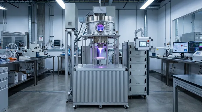
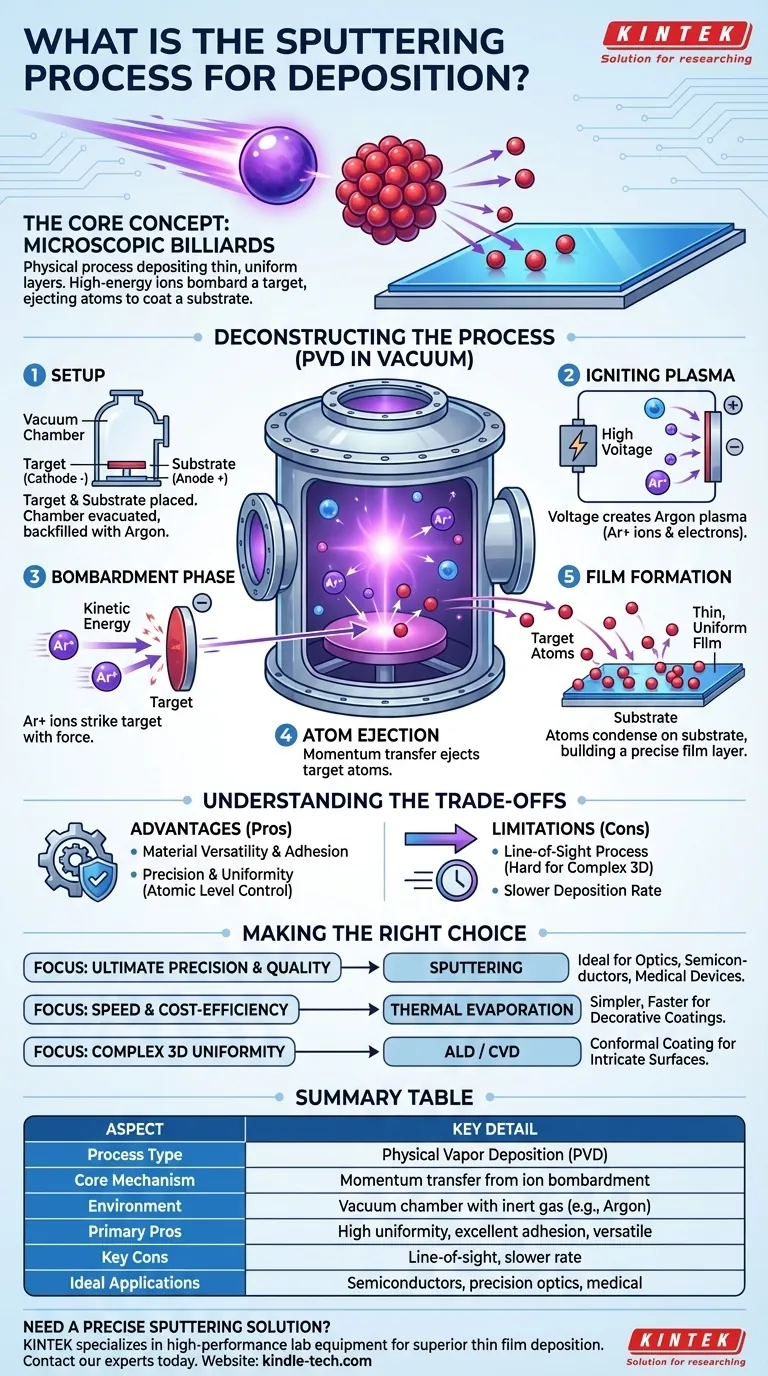
At its core, sputtering is a physical process used to deposit exceptionally thin and uniform layers of material onto a surface. It works by creating a plasma in a vacuum and using the ions from that plasma to bombard a source material, known as a target. This bombardment physically knocks atoms loose from the target, which then travel and coat a nearby object, called a substrate, forming a precise thin film.
Sputtering is not a chemical reaction or a melting process. Think of it as a microscopic game of billiards: high-energy ions act as cue balls, striking atoms in a target material and ejecting them with enough force to travel across a vacuum chamber and stick to a substrate.
Deconstructing the Sputtering Process
Sputtering is a type of Physical Vapor Deposition (PVD). To understand its value, we must break down the mechanics of the process, which occur within a highly controlled vacuum environment.
### The Essential Setup: Chamber and Components
The process begins by placing two key items into a vacuum chamber: the target and the substrate. The target is a solid block of the material you wish to deposit, while the substrate is the object you want to coat.
The chamber is pumped down to a near-perfect vacuum and then backfilled with a small amount of a high-purity inert gas, most commonly Argon.
### Igniting the Plasma
A powerful voltage is applied between the target and the chamber, making the target a negatively charged cathode. This strong electric field energizes the Argon gas, stripping electrons from the Argon atoms.
This creates a plasma, an ionized gas consisting of positively charged Argon ions (Ar+) and free electrons, which typically glows purple or blue.
### The Bombardment Phase
The positively charged Argon ions within the plasma are now powerfully attracted and accelerated toward the negatively charged target.
They strike the target's surface with significant kinetic energy. This is the "sputtering" event—a momentum transfer that is purely physical.
### From Target to Substrate
The energy from the ion impact is sufficient to overcome the binding energy holding the target's surface atoms in place. This sets off a collision cascade within the material.
When this cascade reaches the surface, atoms of the target material are ejected, or "sputtered," into the vacuum chamber. These atoms travel in a vapor stream toward the substrate.
### Film Formation on the Substrate
The ejected target atoms land on the substrate, where they cool, condense, and bond to the surface.
Over time, these atoms build up layer by layer, forming a thin, solid, and highly uniform film. The process allows for precise control over the film's thickness, density, and grain structure.
Understanding the Trade-offs
Sputtering is a powerful technique, but its advantages come with specific limitations. Understanding these trade-offs is crucial for deciding if it is the right process for your application.
### Advantage: Material Versatility and Adhesion
Sputtering can be used to deposit a vast range of materials, including pure metals, alloys, and even insulating ceramic compounds (using a variant called RF sputtering). The high energy of the deposited atoms often results in excellent film adhesion.
### Advantage: Precision and Uniformity
The primary strength of sputtering is its control. By carefully managing gas pressure, voltage, and time, you can achieve films with highly specific thicknesses (down to single angstroms) and uniform properties, which is critical for optical and semiconductor applications.
### Limitation: It's a Line-of-Sight Process
Sputtered atoms travel in a relatively straight line from the target to the substrate. This makes it challenging to uniformly coat complex, three-dimensional objects with hidden surfaces or deep trenches. Substrate rotation is often required to mitigate this.
### Limitation: Deposition Rate
Compared to some other methods like thermal evaporation, sputtering can be a slower process. This is the trade-off for achieving higher-quality, denser, and more uniform films. The need for precise control often prioritizes quality over speed.
Making the Right Choice for Your Goal
Sputtering is one of several deposition techniques, and its suitability depends entirely on your end goal.
- If your primary focus is ultimate precision and film quality: Sputtering offers unmatched control over film thickness, density, and structure, making it ideal for high-performance optics, semiconductors, and medical devices.
- If your primary focus is speed and cost-efficiency for simple coatings: Thermal evaporation is often a faster and simpler alternative for applications like decorative metal coatings on plastics.
- If your primary focus is coating complex 3D objects uniformly: Techniques like Atomic Layer Deposition (ALD) or Chemical Vapor Deposition (CVD) are often superior due to their ability to conformally coat intricate surfaces.
Understanding the fundamental mechanism of sputtering empowers you to select the most effective tool for your specific engineering challenge.
Summary Table:
| Aspect | Key Detail |
|---|---|
| Process Type | Physical Vapor Deposition (PVD) |
| Core Mechanism | Momentum transfer from ion bombardment |
| Typical Environment | Vacuum chamber with inert gas (e.g., Argon) |
| Primary Advantages | High uniformity, excellent adhesion, material versatility |
| Key Limitations | Line-of-sight process, slower deposition rate |
| Ideal Applications | Semiconductors, precision optics, medical coatings |
Need a precise and reliable sputtering solution for your lab?
KINTEK specializes in high-performance lab equipment, including sputtering systems designed for superior thin film deposition. Whether you're working in semiconductor research, optical coating development, or medical device manufacturing, our expertise ensures you get the precision, uniformity, and material versatility your projects demand.
Contact our experts today to discuss how KINTEK's sputtering equipment can enhance your laboratory's capabilities and help you achieve your specific coating goals.
Visual Guide
Related Products
- Split Chamber CVD Tube Furnace with Vacuum Station Chemical Vapor Deposition System Equipment Machine
- Chemical Vapor Deposition CVD Equipment System Chamber Slide PECVD Tube Furnace with Liquid Gasifier PECVD Machine
- HFCVD Machine System Equipment for Drawing Die Nano-Diamond Coating
- Customer Made Versatile CVD Tube Furnace Chemical Vapor Deposition Chamber System Equipment
- RF PECVD System Radio Frequency Plasma-Enhanced Chemical Vapor Deposition RF PECVD
People Also Ask
- How does a CVD tube furnace inhibit the sintering of silver supports? Boost Membrane Durability and Performance
- What is the core function of the CVD deposition furnace? Master Bulk ZnS Production with Precision Control
- What is a split tube furnace? Unlock Unmatched Access for Complex Lab Setups
- What is the function of a tube furnace in CVD SiC synthesis? Achieving Ultra-Pure Silicon Carbide Powders
- What is a CVD tube furnace? A Complete Guide to Thin-Film Deposition


