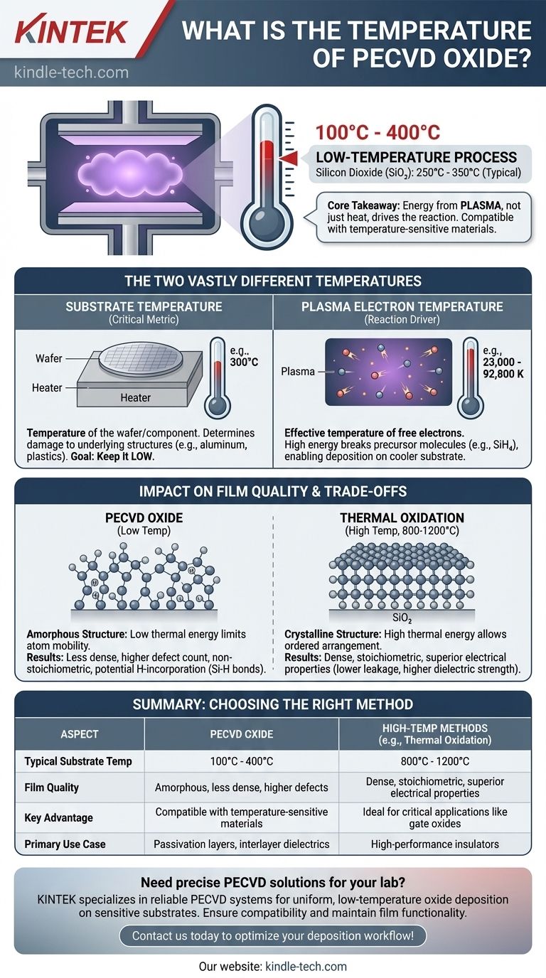
In practice, Plasma-Enhanced Chemical Vapor Deposition (PECVD) for oxide films is a low-temperature process, typically operating with a substrate temperature between 100°C and 400°C. While the exact temperature depends on the specific recipe and desired film properties, a common range for depositing silicon dioxide is 250°C to 350°C. This low thermal budget is the primary reason PECVD is chosen over other methods.
The core takeaway is that PECVD uses energy from a plasma—not just heat—to drive the chemical reaction. This allows for the deposition of functional oxide films at temperatures low enough to be compatible with a wide range of underlying materials, though this comes with a trade-off in film quality compared to high-temperature methods.

The Role of Temperature in PECVD
To understand PECVD, you must distinguish between two vastly different temperatures that exist simultaneously within the reaction chamber. Confusing them is a common but critical mistake.
Substrate Temperature: The Critical Metric
The substrate temperature (e.g., 300°C) is the temperature of the wafer or component you are depositing the film onto. This is the temperature that determines whether underlying structures, such as aluminum interconnects or plastics, will be damaged.
The main advantage of PECVD is keeping this temperature low. This makes it possible to deposit insulating layers late in the manufacturing process, after temperature-sensitive components have already been fabricated.
Plasma Electron Temperature: The Reaction Driver
The plasma itself contains free electrons with extremely high energy. Their effective temperature can be tens of thousands of degrees Kelvin (23,000 to 92,800 K, per the references).
These high-energy electrons collide with the precursor gas molecules (like silane, SiH₄), breaking them apart into reactive fragments. This energy from the plasma, rather than thermal energy, is what enables the deposition reaction to occur on the much cooler substrate surface.
How Temperature Impacts Film Quality
The deposition temperature is a primary lever that controls the final properties of the oxide film. The "low temperature" benefit of PECVD directly leads to its most significant compromises.
The PECVD Film Structure
Because the atoms arriving at the substrate surface have low thermal energy, they have limited mobility. They essentially "stick" where they land, without the energy to rearrange into a perfect, ordered lattice.
This results in a film that is amorphous (lacking a crystalline structure) and often non-stoichiometric, meaning the ratio of silicon to oxygen atoms isn't a perfect 1:2. It is also less dense than a thermally grown oxide.
Comparison with High-Temperature Methods
Methods like thermal oxidation (growing oxide at 800-1200°C) or Low-Pressure CVD (LPCVD) (depositing at 400°C or higher) use heat to drive the reaction.
This high thermal energy allows atoms to find their ideal positions, resulting in a denser, more ordered, and stoichiometric SiO₂ film. These films have superior electrical properties, such as lower leakage current and higher dielectric strength, making them suitable for critical applications like gate oxides in transistors.
Understanding the Trade-offs: Quality vs. Compatibility
Choosing PECVD is always an exercise in balancing the need for a low thermal budget against the requirement for film quality. It is not a universal replacement for other deposition techniques.
The Quality Compromise
A PECVD oxide film is fundamentally inferior to a high-quality thermal oxide. Its lower density and higher defect count make it "leakier" and less robust as an electrical insulator.
For this reason, PECVD oxide is typically used for less demanding roles, such as a passivation layer to protect the chip from the environment or as an interlayer dielectric to insulate metal wiring levels.
The Hydrogen Problem
Many PECVD recipes use hydrogen-containing precursors (e.g., silane). This hydrogen can become incorporated into the deposited film, creating Si-H bonds.
These bonds can be a source of instability, potentially affecting the device's electronic performance over its lifetime. A subsequent annealing step (heating the wafer) is often required to drive out this hydrogen, which adds complexity and thermal budget back into the process.
Making the Right Choice for Your Goal
The decision to use PECVD is driven entirely by the constraints of your fabrication process and the requirements of the specific layer you are creating.
- If your primary focus is the highest quality gate dielectric: You must use thermal oxidation. Its superior electrical properties are non-negotiable for this application, despite the high temperature.
- If your primary focus is depositing an insulator over existing metal lines or other temperature-sensitive layers: PECVD is the correct and often only choice, as its low substrate temperature prevents damage.
- If your primary focus is good film uniformity on many wafers at once (batch processing) with moderate quality: LPCVD can be an excellent middle-ground, offering better quality than PECVD at a lower temperature than thermal oxidation.
Ultimately, understanding the temperature of PECVD is about understanding its core purpose: enabling deposition where high temperatures are simply not an option.
Summary Table:
| Aspect | PECVD Oxide | High-Temperature Methods (e.g., Thermal Oxidation) |
|---|---|---|
| Typical Substrate Temperature | 100°C - 400°C | 800°C - 1200°C |
| Film Quality | Amorphous, less dense, higher defect count | Dense, stoichiometric, superior electrical properties |
| Key Advantage | Compatible with temperature-sensitive materials (e.g., aluminum, plastics) | Ideal for critical applications like gate oxides |
| Primary Use Case | Passivation layers, interlayer dielectrics | High-performance insulators where thermal budget allows |
Need precise PECVD solutions for your lab? KINTEK specializes in lab equipment and consumables, providing reliable PECVD systems that deliver uniform, low-temperature oxide deposition for sensitive substrates. Our expertise ensures compatibility with your fabrication process while maintaining film functionality. Contact us today to optimize your deposition workflow and protect your temperature-sensitive materials!
Visual Guide
Related Products
- Inclined Rotary Plasma Enhanced Chemical Vapor Deposition PECVD Equipment Tube Furnace Machine
- Chemical Vapor Deposition CVD Equipment System Chamber Slide PECVD Tube Furnace with Liquid Gasifier PECVD Machine
- Inclined Rotary Plasma Enhanced Chemical Vapor Deposition PECVD Equipment Tube Furnace Machine
- RF PECVD System Radio Frequency Plasma-Enhanced Chemical Vapor Deposition RF PECVD
- Multi Heating Zones CVD Tube Furnace Machine Chemical Vapor Deposition Chamber System Equipment
People Also Ask
- What are the advantages of plasma enhanced chemical vapor deposition? Enable Low-Temperature, High-Quality Film Deposition
- What are the core advantages of PE-CVD in OLED encapsulation? Protect Sensitive Layers with Low-Temp Film Deposition
- How does plasma enhanced chemical vapor deposition work? Enable Low-Temperature Thin Film Deposition
- How does PECVD facilitate Ru-C nanocomposite films? Precision Low-Temperature Thin Film Synthesis
- What are the benefits of plasma enhanced CVD? Achieve High-Quality, Low-Temperature Film Deposition


