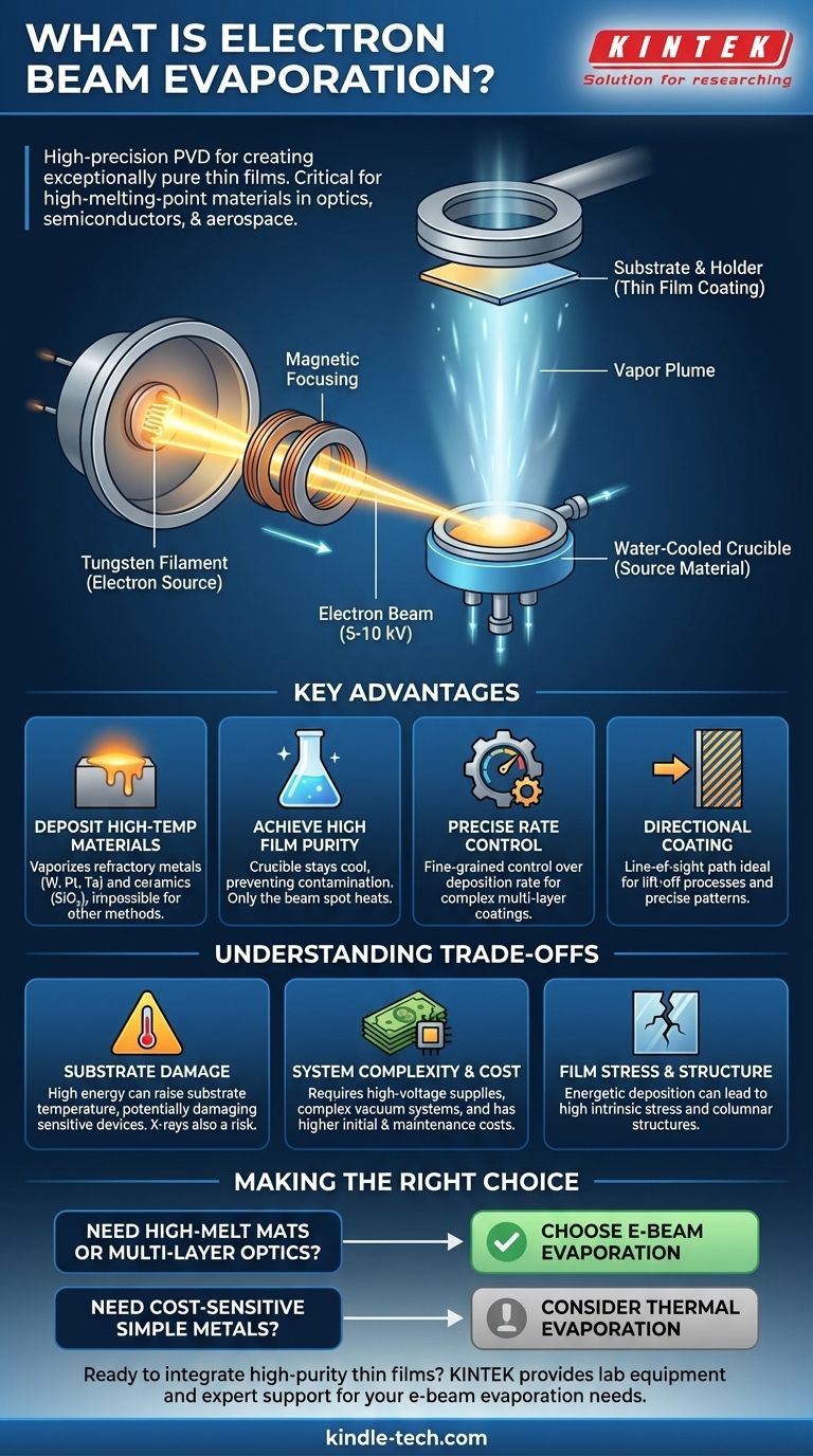
At its core, electron beam evaporation is a high-precision manufacturing technique used to create exceptionally pure and high-performance thin films. It is a form of physical vapor deposition (PVD) where a focused beam of high-energy electrons vaporizes a source material inside a vacuum, which then condenses onto a substrate to form a coating. This method is critical for applications demanding materials with very high melting points, such as in advanced optics, semiconductors, and aerospace components.
The primary reason to use electron beam evaporation is its ability to deposit materials that simpler methods cannot handle. By using a focused electron beam, it achieves extremely high, localized temperatures, enabling the vaporization of refractory metals and dielectric ceramics while maintaining high film purity and precise control over the coating's thickness and properties.
How Does E-Beam Evaporation Work?
Electron beam evaporation is a sophisticated process that relies on fundamental physics to create thin films with remarkable precision. The entire process takes place within a high-vacuum chamber to ensure the purity of the final film.
The Electron Source
A high electrical current is passed through a tungsten filament. This causes the filament to heat up intensely, leading to the thermionic emission of electrons—essentially "boiling" electrons off the metal surface.
The Beam and Target
These free electrons are then accelerated by a high voltage, typically between 5 and 10 kilovolts (kV), giving them significant kinetic energy. A magnetic field is used to precisely focus these high-energy electrons into a narrow beam, directing it toward the source material held in a water-cooled crucible.
The Deposition Process
When the electron beam strikes the source material, the electrons' kinetic energy is instantly converted into intense thermal energy. This localized heating causes the material to rapidly evaporate or sublimate into a vapor. This vapor then travels in a straight, line-of-sight path until it condenses on the cooler substrate, forming a dense and uniform thin film.
Key Advantages Driving Its Use
The "why" behind choosing e-beam evaporation lies in a set of distinct advantages over other deposition techniques, particularly standard thermal evaporation.
Depositing High-Temperature Materials
This is the most significant advantage. Standard thermal evaporators heat an entire boat or crucible, limiting them to materials with lower melting points. E-beam's focused energy can vaporize materials with extremely high melting points, such as platinum, tungsten, tantalum, and ceramics like silicon dioxide (SiO₂), which are impossible to deposit otherwise.
Achieving High Film Purity
Because the source material is held in a water-cooled crucible, only the small spot hit by the electron beam gets superheated. This prevents contamination from the crucible itself, resulting in films of exceptionally high purity compared to methods that heat the entire container.
Enabling Precise Control
The intensity of the electron beam can be adjusted with high precision, allowing for fine-grained control over the deposition rate. This control is critical for creating complex optical coatings or advanced electronic structures where film thickness and density directly determine performance.
Creating Directional Coatings (Line-of-Sight)
The vapor from e-beam evaporation travels in a straight line to the substrate. This directional or "anisotropic" deposition is crucial for semiconductor manufacturing processes like lift-off, where material must be deposited at the bottom of a patterned trench without coating the sidewalls.
Understanding the Trade-offs
No technique is perfect. To make an informed decision, it is crucial to understand the limitations of electron beam evaporation.
Potential for Substrate Damage
The high energy involved in the process isn't limited to the source material. Stray electrons and the heat of condensation can raise the temperature of the substrate, which can damage sensitive materials or devices. Furthermore, the high-energy electrons can generate X-rays, which may degrade certain electronic components.
System Complexity and Cost
E-beam evaporation systems are significantly more complex and expensive than simpler thermal evaporators. They require high-voltage power supplies, sophisticated magnetic focusing systems, and robust vacuum equipment, leading to higher initial investment and maintenance costs.
Film Stress and Structure
The energetic nature of the deposition can sometimes lead to high intrinsic stress within the deposited film, which may cause adhesion problems or mechanical failure. The resulting film structure can also be highly columnar, which may not be desirable for all applications.
Making the Right Choice for Your Application
Selecting the correct deposition method depends entirely on your material requirements, performance goals, and budget.
- If your primary focus is depositing high-melting-point materials like refractory metals or ceramics: Electron beam evaporation is the definitive and often only choice.
- If your primary focus is creating multi-layer optical coatings with precise refractive indices: The rate control and purity of e-beam evaporation are essential for high performance.
- If your primary focus is fabricating patterned metal layers using lift-off: The directional nature of e-beam evaporation is a significant advantage.
- If your primary focus is cost-sensitive deposition of simple metals like aluminum or gold: A simpler and less expensive thermal evaporation system may be a more practical solution.
By understanding its unique capabilities and trade-offs, you can leverage electron beam evaporation to fabricate advanced films that are otherwise impossible to create.
Summary Table:
| Key Feature | Benefit for Your Application |
|---|---|
| High-Temperature Capability | Deposits refractory metals (e.g., Tungsten) and ceramics impossible with other methods. |
| Exceptional Purity | Water-cooled crucible prevents contamination, ensuring high-performance films. |
| Precise Rate Control | Enables accurate, repeatable film thickness for complex optical and electronic layers. |
| Directional Coating | Ideal for semiconductor lift-off processes and precise pattern definition. |
Ready to integrate high-purity thin films into your lab's workflow?
Electron beam evaporation is essential for R&D and production requiring the highest material performance. KINTEK specializes in providing the lab equipment and expert support to help you leverage this advanced technology.
Contact our experts today to discuss how our e-beam evaporation solutions can meet your specific application needs for semiconductors, optics, and aerospace components.
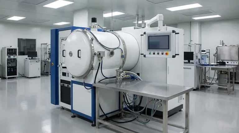
Visual Guide
Related Products
- Electron Beam Evaporation Coating Tungsten Crucible and Molybdenum Crucible for High Temperature Applications
- Electron Beam Evaporation Coating Oxygen-Free Copper Crucible and Evaporation Boat
- Electron Beam Evaporation Coating Gold Plating Tungsten Molybdenum Crucible for Evaporation
- Electron Beam Evaporation Coating Conductive Boron Nitride Crucible BN Crucible
- E Beam Crucibles Electron Gun Beam Crucible for Evaporation
People Also Ask
- What is e-beam evaporation used for? Precision Coating for Optics, Aerospace & Electronics
- What materials are used in electron beam evaporation? Master High-Purity Thin Film Deposition
- What is the container that holds the metal source material called in e-beam evaporation? Ensure Purity and Quality in Your Thin-Film Deposition
- What is e-beam evaporation? Achieve High-Purity Thin Film Deposition for Your Lab
- What is the voltage of e-beam evaporation? Achieve Precise Thin-Film Deposition


