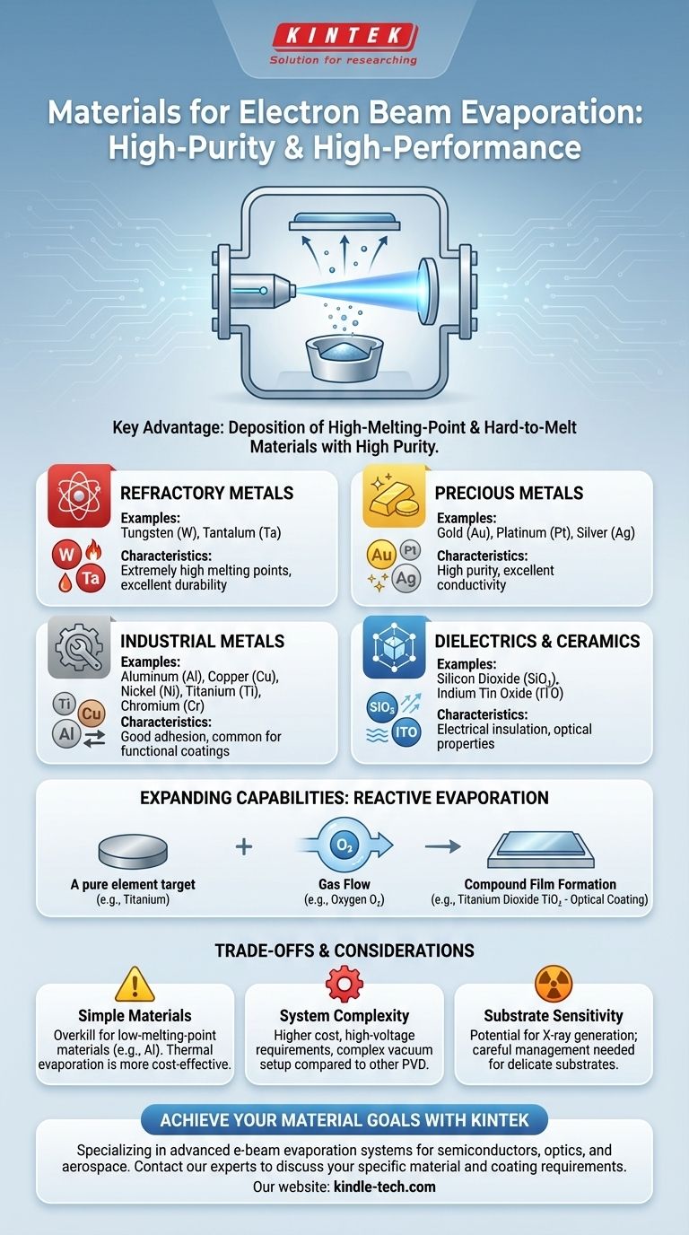
In short, electron beam evaporation excels at depositing materials with high melting points. It is commonly used for a wide range of substances, including refractory metals like tungsten and tantalum, precious metals like gold and platinum, and dielectric compounds such as silicon dioxide.
The core advantage of electron beam (e-beam) evaporation is its ability to use a highly concentrated energy beam to vaporize materials that are impossible or impractical to melt with other methods. This makes it the premier choice for creating dense, high-purity thin films from a vast catalog of elements and compounds.
Why E-Beam Excels with Demanding Materials
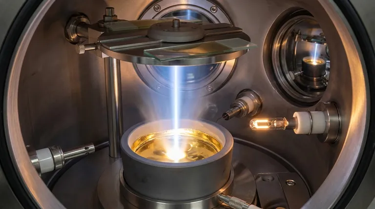
Electron beam evaporation is a form of physical vapor deposition (PVD) that operates under a high vacuum. Its unique capabilities stem directly from its method of energy delivery.
The Principle of Concentrated Energy
Unlike traditional thermal evaporation, which heats an entire crucible to melt the source material, an e-beam directs a focused stream of high-energy electrons directly onto the target.
This converts the electrons' kinetic energy into intense thermal energy in a very small area. This localized heating is efficient enough to melt and vaporize materials with extremely high melting temperatures.
Preserving Material Purity
Because the electron beam only heats the source material itself, it minimizes contact and reaction with the crucible holding it.
This direct heating process significantly reduces the risk of contamination, resulting in high-purity films that are critical for applications in optics, semiconductors, and aerospace.
A Gallery of Compatible Materials
E-beam's power makes it compatible with a diverse set of materials that are crucial for modern technology.
Refractory & Precious Metals
These materials are defined by their high melting points and resistance to degradation. E-beam is one of the few reliable methods for depositing them.
- Tungsten (W)
- Tantalum (Ta)
- Platinum (Pt)
- Gold (Au)
- Silver (Ag)
Common Industrial Metals
While some of these can be deposited by other means, e-beam provides superior density and purity.
- Aluminum (Al)
- Copper (Cu)
- Nickel (Ni)
- Titanium (Ti)
- Chromium (Cr)
Dielectrics & Ceramics
These non-conductive materials are fundamental to optical coatings and electronics.
- Silicon Dioxide (SiO₂)
- Indium Tin Oxide (ITO)
Expanding Capabilities with Reactive Evaporation
The versatility of e-beam evaporation is not limited to pure elements. The process can be adapted to create compound films.
Beyond Pure Elements
By introducing a controlled flow of a specific gas into the vacuum chamber during deposition, a chemical reaction can be triggered. This process is known as reactive evaporation.
Forming Compound Films
For example, a pure titanium target can be evaporated in the presence of oxygen gas. The vaporized titanium atoms react with the oxygen on their way to the substrate, forming a film of **titanium dioxide (TiO₂) **, a common optical coating. This method is used to create a wide variety of oxides, nitrides, and other compound films.
Understanding the Trade-offs
While powerful, e-beam evaporation is not a universal solution. It's essential to understand its specific context and limitations.
Overkill for Simpler Materials
For materials with low melting points, such as aluminum or tin, simpler and more cost-effective methods like thermal evaporation are often sufficient.
System Complexity and Cost
E-beam systems require a high-voltage power supply, magnetic coils for beam steering, and a sophisticated vacuum setup. This makes them inherently more complex and expensive than other PVD technologies.
Potential for Substrate Damage
The high-energy electrons can generate secondary radiation, including X-rays, upon impact with the source material. For highly sensitive substrates, such as certain biological samples or delicate electronics, this can be a source of potential damage that must be managed.
Making the Right Choice for Your Application
Selecting the right deposition technique depends entirely on your material requirements and performance goals.
- If your primary focus is high-purity, refractory metal coatings: E-beam evaporation is the definitive choice for its ability to handle materials like tungsten and tantalum.
- If your primary focus is complex optical coatings: E-beam, often combined with reactive evaporation, provides the precision needed to deposit high-quality dielectric layers like SiO₂ and TiO₂.
- If your primary focus is simple, low-temperature metal films: A less complex method like thermal evaporation may be a more cost-effective solution.
Ultimately, electron beam evaporation provides a uniquely powerful and versatile tool for depositing a vast range of high-performance materials that are foundational to advanced engineering.
Summary Table:
| Material Category | Common Examples | Key Characteristics |
|---|---|---|
| Refractory Metals | Tungsten (W), Tantalum (Ta) | Extremely high melting points, excellent durability |
| Precious Metals | Gold (Au), Platinum (Pt), Silver (Ag) | High purity, excellent conductivity |
| Industrial Metals | Aluminum (Al), Copper (Cu), Titanium (Ti) | Good adhesion, common for functional coatings |
| Dielectrics & Ceramics | Silicon Dioxide (SiO₂), Indium Tin Oxide (ITO) | Electrical insulation, optical properties |
Need to deposit high-purity materials like tungsten, gold, or silicon dioxide?
KINTEK specializes in advanced lab equipment, including electron beam evaporation systems, to help you achieve dense, high-performance thin films for your most demanding applications in semiconductors, optics, and aerospace. Our expertise ensures you get the right solution for your specific material and coating requirements.
Contact our experts today to discuss how our e-beam evaporation technology can enhance your research and production.
Visual Guide
Related Products
- Electron Beam Evaporation Coating Tungsten Crucible and Molybdenum Crucible for High Temperature Applications
- Electron Beam Evaporation Coating Gold Plating Tungsten Molybdenum Crucible for Evaporation
- High Purity Pure Graphite Crucible for Electron Beam Evaporation
- Electron Beam Evaporation Coating Conductive Boron Nitride Crucible BN Crucible
- Electron Beam Evaporation Coating Oxygen-Free Copper Crucible and Evaporation Boat
People Also Ask
- What is e-beam evaporation used for? Precision Coating for Optics, Aerospace & Electronics
- What is the deposition rate of e-beam evaporation? Control Thin Film Quality and Speed
- What is the current of e-beam evaporation? A Guide to High-Purity Thin Film Deposition
- What is the voltage of e-beam evaporation? Achieve Precise Thin-Film Deposition
- What is the process of e-beam coating? Achieve High-Purity, Precise Thin Films for Your Lab


