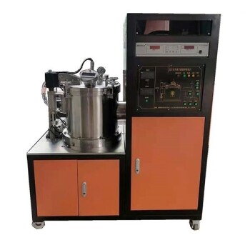
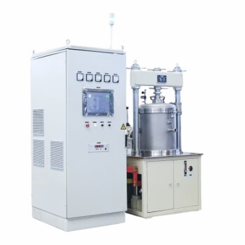
In simple terms, vacuum evaporation is a method for applying a very thin coating of one material onto another. Inside a high-vacuum chamber, the coating material is heated until it turns into a vapor, which then travels and condenses onto the target object, forming a solid, uniform film.
The central concept to grasp is that vacuum evaporation is one of the most fundamental types of Physical Vapor Deposition (PVD). It achieves coating through a straightforward physical process: changing a material from a solid to a vapor and back to a solid, all within a vacuum.
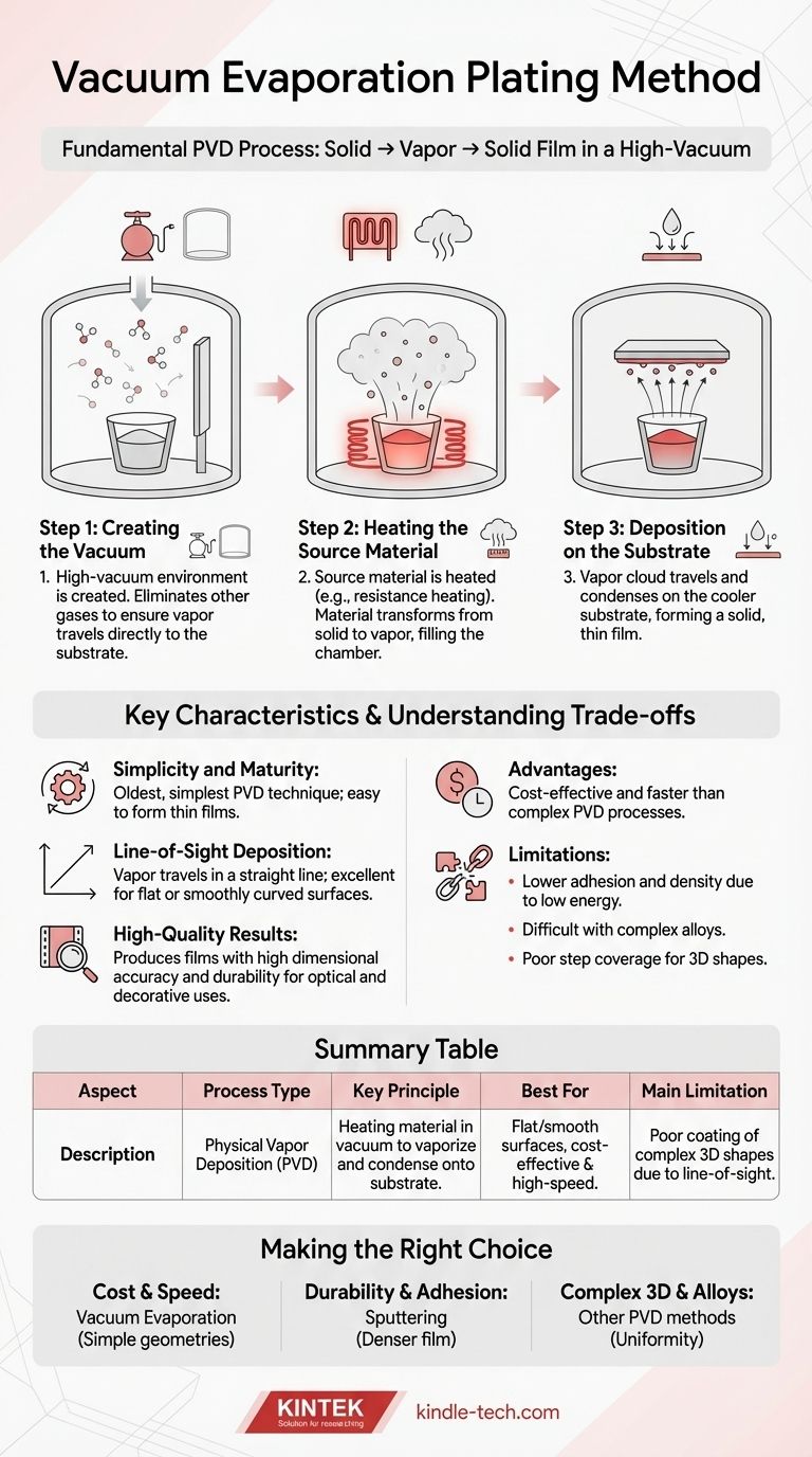
The Fundamental Process: From Solid to Film
To understand how vacuum evaporation works, it's best to break it down into its three critical stages. The entire process relies on controlling the physical state of the coating material.
Creating the Vacuum
The first step is to place the source material and the object to be coated (the substrate) into a chamber and remove almost all of the air.
This high-vacuum environment is crucial because it eliminates other gas atoms. This ensures the vaporized coating material can travel directly to the substrate without colliding with anything along the way.
Heating the Source Material
Once the vacuum is established, the source material is heated. This is often done using resistance heating, where a large electrical current is passed through the material, causing it to heat up rapidly.
As the material reaches its evaporation point, it transforms from a solid or liquid into a gas, or vapor, filling the chamber.
Deposition on the Substrate
This cloud of vapor travels through the vacuum and makes contact with the cooler surface of the substrate.
Much like steam from a hot shower condenses on a cold mirror, the vaporized material instantly condenses back into a solid state upon hitting the substrate, forming a thin, even film.
Key Characteristics of the Method
Vacuum evaporation is a well-established process with distinct characteristics that define its use cases.
Simplicity and Maturity
As one of the oldest and simplest PVD techniques, the equipment and process are straightforward and well-understood. It is often considered the easiest way to form a thin film.
Line-of-Sight Deposition
The vaporized atoms travel in a relatively straight line from the source to the substrate. This means the process is excellent for coating flat or smoothly curved surfaces that directly face the source.
High-Quality Results
When properly controlled, this method can produce films with high dimensional accuracy and durability for a variety of applications, from optical lenses to decorative finishes.
Understanding the Trade-offs
No single process is perfect for every application. The simplicity of vacuum evaporation comes with specific limitations you must consider.
Advantage: Cost and Speed
The relative simplicity of the equipment often makes vacuum evaporation a more cost-effective and faster deposition method compared to more complex PVD processes like sputtering.
Limitation: Adhesion and Density
Because the vapor atoms arrive at the substrate with relatively low energy, the resulting films may have lower density and weaker adhesion compared to films produced by higher-energy methods.
Limitation: Material Constraints
The process is best suited for materials that evaporate cleanly at a reasonable temperature. Attempting to evaporate complex alloys can be difficult, as different elements within the alloy may evaporate at different rates, changing the composition of the final film.
Limitation: Step Coverage
Due to its line-of-sight nature, vacuum evaporation is not effective at coating complex, three-dimensional shapes with sharp edges, holes, or undercuts. Areas not in the direct path of the vapor will receive little to no coating.
Making the Right Choice for Your Goal
Selecting the right coating method requires matching the process capabilities to your desired outcome.
- If your primary focus is cost-effective coating for simple geometries: Vacuum evaporation is an excellent and highly efficient choice, especially for decorative or optical applications.
- If your primary focus is maximum film durability and adhesion: You should investigate higher-energy deposition methods like sputtering, which create a denser and more strongly bonded film.
- If your primary focus is coating complex 3D parts or specific alloys: The limitations of vacuum evaporation make other processes a more suitable choice for achieving a uniform and compositionally accurate coating.
Understanding these core principles allows you to select the right coating technology for your specific engineering challenge.
Summary Table:
| Aspect | Description |
|---|---|
| Process Type | Physical Vapor Deposition (PVD) |
| Key Principle | Heating a material in a vacuum to vaporize it, then condensing it onto a substrate. |
| Best For | Flat/smooth surfaces, cost-effective & high-speed deposition. |
| Main Limitation | Poor coating of complex 3D shapes due to line-of-sight deposition. |
Need a reliable thin film coating solution for your lab or production line?
At KINTEK, we specialize in lab equipment and consumables, including vacuum evaporation systems. Whether you're working on optical coatings, decorative finishes, or R&D projects, our experts can help you select the right PVD technology to achieve high-quality, durable results efficiently.
Contact our team today to discuss your specific requirements and discover how KINTEK's solutions can enhance your coating process.
Visual Guide
Related Products
- Electron Beam Evaporation Coating Gold Plating Tungsten Molybdenum Crucible for Evaporation
- Molybdenum Tungsten Tantalum Evaporation Boat for High Temperature Applications
- Molybdenum Tungsten Tantalum Special Shape Evaporation Boat
- Vacuum Cold Mounting Machine for Sample Preparation
- High Purity Pure Graphite Crucible for Evaporation
People Also Ask
- What materials are used in electron beam evaporation? Master High-Purity Thin Film Deposition
- What are the applications of e-beam evaporation? Achieve High-Purity Coatings for Optics & Electronics
- What is e-beam evaporation? Achieve High-Purity Thin Film Deposition for Your Lab
- What is the voltage of e-beam evaporation? Achieve Precise Thin-Film Deposition
- What is e-beam evaporation used for? Precision Coating for Optics, Aerospace & Electronics