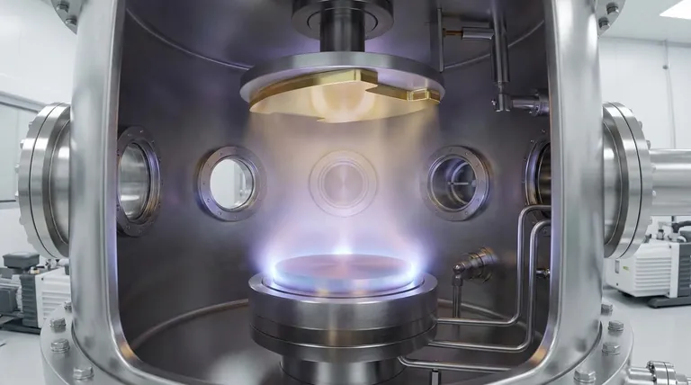
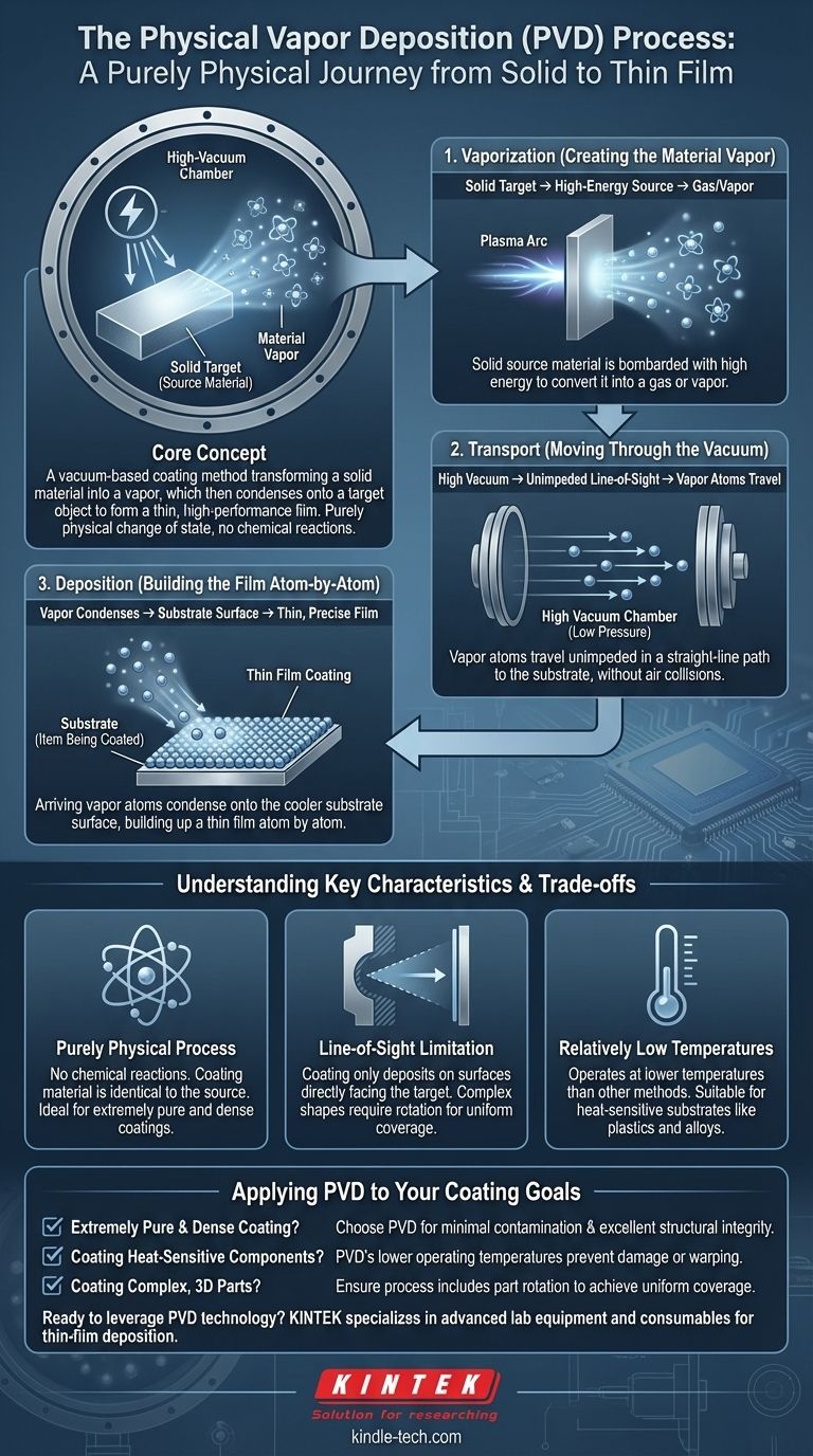
At its core, Physical Vapor Deposition (PVD) is a vacuum-based coating method that transforms a solid material into a vapor, which then condenses onto a target object to form a thin, high-performance film. This entire process is purely physical, involving a change of state from solid to gas and back to solid, with no chemical reactions occurring. The coating is built meticulously, one atom or molecule at a time.
The central concept of PVD involves three fundamental stages conducted in a high-vacuum chamber: a solid source material is vaporized using energy, the resulting vapor travels unimpeded to the substrate, and it then condenses on the substrate's surface to form the desired thin film.
The Fundamental PVD Process: A Three-Step Journey
To truly understand how PVD works, it's best to break it down into its three distinct, sequential phases. Each step is critical for producing a high-quality, uniform coating.
Step 1: Vaporization (Creating the Material Vapor)
The process begins with the source material, known as the target, which is in a solid form. The goal is to convert this solid into a gas or vapor.
This is accomplished by bombarding the target with a high-energy source. Different PVD methods are categorized by how they achieve this, using techniques like high-temperature evaporation or blasting the surface with high-energy particles from sources like a plasma or an electron beam.
Step 2: Transport (Moving Through the Vacuum)
Once the target material is vaporized, its atoms or molecules travel through the process chamber. This journey happens in a high vacuum, an environment with extremely low pressure.
The vacuum is essential because it removes air and other particles that could collide with the vaporized material. This ensures the material travels in a straight, unimpeded path—often referred to as line-of-sight—from the target to the object being coated.
Step 3: Deposition (Building the Film Atom-by-Atom)
When the vaporized atoms arrive at the surface of the item being coated (the substrate), they condense back into a solid state.
Because the substrate is typically at a lower temperature, the arriving vapor atoms settle onto its surface, creating a thin, dense, and highly adherent film. This layer builds up atom by atom, allowing for extremely precise control over its thickness and structure.
Understanding the Trade-offs and Key Characteristics
While powerful, the PVD process has distinct characteristics and limitations that are important to understand for its proper application.
A Purely Physical Process
One of the defining features of PVD is that no chemical reactions take place. The coating material is the same as the source material, just deposited in a thin layer. This is a primary differentiator from processes like Chemical Vapor Deposition (CVD), where chemical reactions on the substrate surface form the coating.
The Line-of-Sight Limitation
The straight-line path of the vaporized material means that surfaces not directly in the "line-of-sight" of the source target will not be coated effectively. To achieve a uniform coating on complex shapes, the substrates must often be rotated or repositioned during the process.
Relatively Low Temperatures
PVD is considered a "cold" process compared to many other coating methods. The lower temperatures make it suitable for a wide range of substrates, including some plastics and finely-tuned metal alloys that could be damaged by high-heat treatments.
Applying This to Your Coating Goal
Understanding the core principles of PVD helps you determine if it's the right choice for your specific application.
- If your primary focus is an extremely pure and dense coating: The high-vacuum environment and physical deposition of PVD are ideal for creating films with minimal contamination and excellent structural integrity.
- If your primary focus is coating heat-sensitive components: PVD's lower operating temperatures make it a superior choice over high-heat alternatives that could damage or warp the substrate.
- If your primary focus is coating a complex, three-dimensional part: You must account for the line-of-sight nature of PVD and ensure the process includes mechanisms for part rotation to achieve uniform coverage.
By grasping these fundamentals, you can better leverage the precision and versatility of the PVD process.
Summary Table:
| PVD Process Stage | Key Action | Crucial Condition |
|---|---|---|
| 1. Vaporization | Solid target material is converted into a vapor. | High-energy source (e.g., plasma, electron beam). |
| 2. Transport | Vapor travels from target to substrate. | High-vacuum environment for unimpeded, line-of-sight travel. |
| 3. Deposition | Vapor condenses on the substrate surface, forming a thin film. | Substrate at a lower temperature for atom-by-atom buildup. |
| Key Characteristic | Description | Consideration |
| Purely Physical | No chemical reactions; coating material is identical to the source. | Ideal for creating extremely pure and dense coatings. |
| Line-of-Sight | Coating only deposits on surfaces directly facing the target. | Complex parts require rotation for uniform coverage. |
| Low Temperature | Operates at relatively low temperatures compared to other methods. | Suitable for heat-sensitive substrates like plastics and alloys. |
Ready to leverage PVD technology for your precision coating needs?
KINTEK specializes in providing advanced lab equipment and consumables for thin-film deposition and materials science. Whether you are developing new coatings for cutting tools, medical devices, or electronic components, our expertise can help you achieve superior results.
Contact our experts today to discuss how our solutions can enhance your laboratory's capabilities and drive your research and development forward.
Visual Guide
Related Products
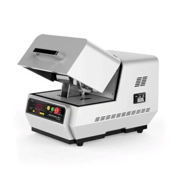
- Vacuum Hot Press Furnace Machine for Lamination and Heating
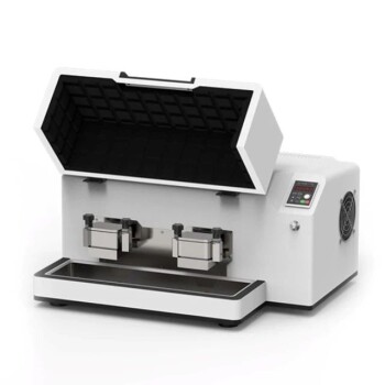
- HFCVD Machine System Equipment for Drawing Die Nano-Diamond Coating
- 915MHz MPCVD Diamond Machine Microwave Plasma Chemical Vapor Deposition System Reactor
- Laboratory Sterilizer Lab Autoclave Pulse Vacuum Lifting Sterilizer
- Laboratory Sterilizer Lab Autoclave Vertical Pressure Steam Sterilizer for Liquid Crystal Display Automatic Type
People Also Ask
- What are the advantages and disadvantages of hot pressing? Choose the Right Powder Metallurgy Process
- How does hot pressing work? Achieve Maximum Density for Advanced Materials
- What is the main function of hot press forming? Achieve Superior Strength & Precision in Manufacturing
- What is the advantage by using hot press forming? Achieve Stronger, More Complex Parts
- What is hot press forging? Creating Complex, High-Strength Metal Components