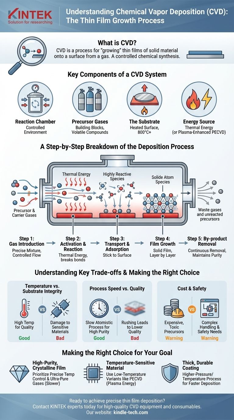
In essence, Chemical Vapor Deposition (CVD) is a process for "growing" thin films of solid material onto a surface from a gas. Precursor gases containing the required chemical elements are introduced into a reaction chamber. There, they are exposed to high energy, typically from a heated substrate, which triggers a chemical reaction that deposits a solid layer onto that substrate, atom by atom.
At its core, CVD is not merely a coating process but a controlled chemical synthesis. It transforms carefully selected gases into a solid, high-purity film on a surface by using thermal energy to drive specific chemical reactions. The quality of the final film is dictated entirely by how well you control the temperature, pressure, and gas chemistry inside the chamber.
The Key Components of a CVD System
To understand the process, you must first understand its essential components. Every CVD system, regardless of its specific type, is built around these four elements.
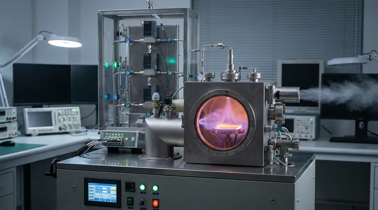
The Reaction Chamber
This is the sealed, controlled environment where the entire process takes place. It is designed to maintain a specific pressure and to prevent contamination from the outside atmosphere.
Precursor Gases
These are the "building blocks" of the film. Precursors are volatile chemical compounds that exist as gases at or near room temperature and contain the atoms you wish to deposit (e.g., methane gas, CH₄, as a source of carbon for diamond films). They are often mixed with inert carrier gases that help transport them into the chamber.
The Substrate
This is the material or wafer onto which the thin film is grown. The substrate is placed on a holder, or "susceptor," which is heated to a precise, high temperature (often 800°C or higher). This heat provides the critical energy for the chemical reaction.
The Energy Source
While the heated substrate is the most common energy source, some CVD variants use other methods. Plasma-Enhanced CVD (PECVD), for instance, uses an RF plasma field to break down gases at lower temperatures, making it suitable for substrates that cannot withstand extreme heat.
A Step-by-Step Breakdown of the Deposition Process
The CVD process can be understood as a sequence of five distinct physical and chemical events.
Step 1: Gas Introduction
A precise mixture of precursor and carrier gases is introduced into the reaction chamber at a controlled flow rate.
Step 2: Activation and Reaction
As the gases flow over or near the hot substrate, the thermal energy breaks their chemical bonds. This creates highly reactive atoms, molecules, and radicals. These reactive species then undergo chemical reactions in the gas phase near the substrate's surface.
Step 3: Transport and Adsorption
The newly formed chemical species diffuse through the gas and land on the hot substrate surface, a process known as adsorption. They stick to the surface but may still have enough energy to move around slightly.
Step 4: Film Growth
On the surface, the adsorbed species find stable sites and form strong chemical bonds with the substrate and with each other. This builds the solid film, layer by layer. The substrate itself can act as a catalyst, making the film adhere strongly.
Step 5: By-product Removal
The chemical reactions produce waste gases as by-products. These, along with any unreacted precursor gases, are continuously pumped out of the chamber through an exhaust system.
Understanding the Key Trade-offs
CVD is a powerful technique, but its effectiveness depends on managing several critical trade-offs. It is not a universally perfect solution.
Temperature vs. Substrate Integrity
The high temperatures required for many CVD processes produce high-quality, crystalline films. However, this same heat can damage or destroy thermally sensitive substrates, such as plastics or certain electronic components.
Process Speed vs. Quality
Achieving a highly ordered, pure crystalline structure (like a lab-grown diamond) is an atomistic process that can be extremely slow, sometimes taking days or weeks. Rushing the process by increasing gas flow or pressure often leads to lower-quality, amorphous, or contaminated films.
Cost and Safety
The precursor gases used in CVD can be expensive, highly toxic, flammable, or corrosive. This necessitates complex and costly gas handling and safety systems, adding to the overall expense and operational complexity.
Making the Right Choice for Your Goal
The specific parameters of the CVD process must be tuned to your final objective.
- If your primary focus is a high-purity, crystalline film (e.g., for semiconductors or optics): You must prioritize precise control over high temperatures and use ultra-pure precursor gases, accepting a slower deposition rate.
- If your primary focus is depositing a film on a temperature-sensitive material: You must use a low-temperature variant like Plasma-Enhanced CVD (PECVD), which uses plasma energy to activate the gases instead of just heat.
- If your primary focus is a thick, durable, protective coating: A higher-pressure, higher-temperature CVD process is often ideal, as it generally allows for faster deposition rates to build thickness quickly.
Ultimately, mastering CVD is about mastering the chemistry within the chamber to build your desired material from the ground up.
Summary Table:
| Process Step | Key Action | Purpose |
|---|---|---|
| 1. Gas Introduction | Precursor gases enter the chamber | Deliver chemical building blocks |
| 2. Activation & Reaction | Heat/energy breaks gas bonds | Create reactive species for deposition |
| 3. Transport & Adsorption | Species diffuse and stick to substrate | Initiate surface bonding |
| 4. Film Growth | Atoms bond to form solid layer | Build the thin film structure |
| 5. By-product Removal | Waste gases are pumped out | Maintain chamber purity and process control |
Ready to achieve precise thin film deposition in your lab? KINTEK specializes in high-quality CVD equipment and consumables, delivering the control and reliability your laboratory needs for semiconductor, optical, and protective coating applications. Contact our experts today to discuss how our solutions can optimize your CVD process and enhance your research outcomes!
Visual Guide
Related Products
- Chemical Vapor Deposition CVD Equipment System Chamber Slide PECVD Tube Furnace with Liquid Gasifier PECVD Machine
- Customer Made Versatile CVD Tube Furnace Chemical Vapor Deposition Chamber System Equipment
- Microwave Plasma Chemical Vapor Deposition MPCVD Machine System Reactor for Lab and Diamond Growth
- Multi Heating Zones CVD Tube Furnace Machine Chemical Vapor Deposition Chamber System Equipment
- Split Chamber CVD Tube Furnace with Vacuum Station Chemical Vapor Deposition System Equipment Machine
People Also Ask
- What are the core advantages of PE-CVD in OLED encapsulation? Protect Sensitive Layers with Low-Temp Film Deposition
- What are the advantages of chemical vapor deposition? Achieve Superior Thin Films for Your Lab
- How are carbon nanotubes grown? Master Scalable Production with Chemical Vapor Deposition
- What types of substrates are used in CVD to facilitate graphene films? Optimize Graphene Growth with the Right Catalyst
- What is the chemical vapor deposition growth process? Build Superior Thin Films from the Atom Up


