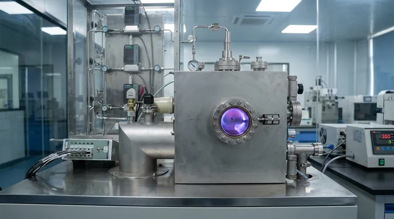
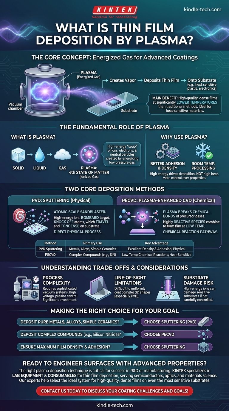
In plasma-based thin film deposition, an energized gas, or plasma, is the primary tool used to create a vapor of coating material and deposit it as an extremely thin layer onto a substrate's surface. This technique is a crucial sub-category of the two main deposition families, Physical Vapor Deposition (PVD) and Chemical Vapor Deposition (CVD), and is performed inside a highly controlled vacuum chamber. The use of plasma enables the creation of high-performance coatings that modify the substrate's electrical, optical, or mechanical properties.
The core advantage of using plasma is its ability to create high-quality, dense films at significantly lower temperatures than traditional thermal methods. This critical feature allows for the advanced coating of heat-sensitive materials like plastics, polymers, and complex electronic components without causing damage.
The Fundamental Role of Plasma
To understand plasma deposition, you must first understand why plasma is used at all. It is not just an alternative; it is an enabling technology for creating materials and properties that are otherwise difficult or impossible to achieve.
What Exactly is Plasma?
Plasma is often called the fourth state of matter, following solid, liquid, and gas. It is created by applying a strong electrical field to a low-pressure gas, which energizes the gas atoms and strips away their electrons.
The result is an ionized gas—a highly reactive mixture of positive ions, electrons, and neutral particles. This energized "soup" of particles can be precisely manipulated with electric and magnetic fields to perform work at the atomic level.
Why Use Plasma for Deposition?
Using a plasma environment provides distinct advantages over purely thermal processes. The high energy of the plasma particles, rather than high heat, drives the deposition.
This results in better film adhesion to the substrate, higher film density, and more control over the final film properties like hardness, stress, and stoichiometry. Most importantly, it allows the entire process to run at or near room temperature.
Two Core Plasma Deposition Methods
While there are many variations, most industrial plasma deposition techniques fall into two primary categories. The choice between them depends entirely on the desired film material and its required properties.
Physical Vapor Deposition (PVD): Sputtering
In sputtering, the plasma's role is purely physical. High-energy ions from the plasma are accelerated and directed at a source material, known as the "target."
Think of this as an atomic-scale sandblaster. The ions bombard the target with such force that they knock off, or "sputter," individual atoms. These vaporized atoms then travel through the vacuum chamber and condense on the substrate, building the thin film one atom at a time.
Plasma-Enhanced Chemical Vapor Deposition (PECVD)
In PECVD, the plasma's role is chemical. Precursor gases are introduced into the vacuum chamber, but unlike traditional CVD, they are not broken down by high heat.
Instead, the energy from the plasma is used to break the chemical bonds in the precursor gases. This creates highly reactive chemical species that then combine on the substrate surface, forming a solid thin film. This avoids the thousands of degrees of heat often required in thermal CVD.
Understanding the Trade-offs and Considerations
While powerful, plasma-based deposition is a complex process with specific requirements and limitations that must be respected for a successful outcome.
Process Complexity
These are not simple benchtop procedures. Plasma deposition requires sophisticated vacuum systems, high-voltage power supplies, and precise mass-flow controllers for the gases. The equipment is a significant capital investment and requires specialized knowledge to operate and maintain.
Line-of-Sight Limitations
In PVD processes like sputtering, deposition is largely a line-of-sight phenomenon. The sputtered atoms travel in relatively straight lines, which can make it difficult to uniformly coat complex, three-dimensional shapes with sharp corners or deep trenches.
Potential for Substrate Damage
While plasma enables low-temperature processing, the high-energy ions can still cause damage to extremely sensitive substrates if the process is not carefully controlled. Managing ion energy is a critical parameter in optimizing any plasma deposition process.
Making the Right Choice for Your Goal
The decision to use a specific plasma technique is dictated by the end goal—the material you need to deposit and the properties you need to achieve.
- If your primary focus is depositing pure metals, alloys, or certain simple ceramics: Sputtering (PVD) is often the most direct and reliable method due to its physical nature.
- If your primary focus is depositing complex dielectric or semiconducting compounds like silicon nitride or amorphous silicon: PECVD provides the chemical reaction pathway needed to form these materials at low temperatures.
- If your primary focus is ensuring maximum film density and adhesion on a durable substrate: Sputtering is an excellent choice, as the energetic arrival of atoms promotes a dense film structure.
By understanding the distinct roles of plasma, you can select the precise deposition technique needed to engineer surfaces with advanced and highly specific properties.
Summary Table:
| Method | Primary Use | Key Advantage |
|---|---|---|
| PVD Sputtering | Depositing pure metals, alloys, simple ceramics | Excellent film density and adhesion; direct physical process |
| PECVD | Depositing complex compounds (e.g., silicon nitride) | Low-temperature chemical reactions; ideal for heat-sensitive materials |
Ready to engineer surfaces with advanced properties? The right plasma deposition technique is critical for your success in R&D or manufacturing. KINTEK specializes in lab equipment and consumables for thin film deposition, serving laboratories in semiconductors, optics, and materials science. Our experts can help you select the ideal system for depositing high-quality, dense films on even the most sensitive substrates. Contact us today to discuss your specific coating challenges and goals!
Visual Guide
Related Products
- Chemical Vapor Deposition CVD Equipment System Chamber Slide PECVD Tube Furnace with Liquid Gasifier PECVD Machine
- 915MHz MPCVD Diamond Machine Microwave Plasma Chemical Vapor Deposition System Reactor
- RF PECVD System Radio Frequency Plasma-Enhanced Chemical Vapor Deposition RF PECVD
- Microwave Plasma Chemical Vapor Deposition MPCVD Machine System Reactor for Lab and Diamond Growth
- Cylindrical Resonator MPCVD Machine System Reactor for Microwave Plasma Chemical Vapor Deposition and Lab Diamond Growth
People Also Ask
- What happens during deposition chemistry? Building Thin Films from Gaseous Precursors
- What is plasma enhanced chemical vapor deposition PECVD equipment? A Guide to Low-Temperature Thin Film Deposition
- What are the advantages of chemical vapor deposition? Achieve Superior Thin Films for Your Lab
- How expensive is chemical vapor deposition? Understanding the True Cost of High-Performance Coating
- What are the core advantages of PE-CVD in OLED encapsulation? Protect Sensitive Layers with Low-Temp Film Deposition


