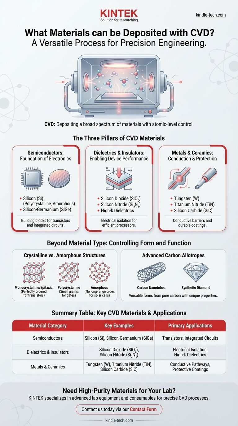
At its core, Chemical Vapor Deposition (CVD) is a process capable of depositing an exceptionally broad spectrum of materials. This includes the three primary categories essential to modern technology: semiconductors like silicon, dielectrics such as silicon nitride, and metals including tungsten. This versatility allows CVD to be used for everything from creating microchips to coating industrial turbine blades.
The true power of CVD is not merely the wide variety of materials it can deposit, but its precise control over the material's final form—be it crystalline, amorphous, or epitaxial. This atomic-level control is what makes CVD a foundational process in microfabrication and advanced materials science.
The Three Pillars of CVD Materials
CVD's versatility can be understood by examining the three main classes of materials it is used to produce. Each class serves a distinct and critical function in technology and industry.
Semiconductors: The Foundation of Electronics
Semiconductors are the bedrock of all modern electronics. CVD is the primary method for depositing these crucial materials onto wafers.
Key examples include silicon (Si) in its various forms (polycrystalline, amorphous) and compound semiconductors like silicon-germanium (SiGe). These films are the building blocks for transistors, memory cells, and other components within integrated circuits.
Dielectrics and Insulators: Enabling Device Performance
For a circuit to function, conductive components must be electrically isolated from one another. CVD excels at creating thin, high-quality insulating films, known as dielectrics.
Common dielectrics include silicon dioxide (SiO₂), silicon nitride (Si₃N₄), and silicon oxynitride (SiON). Advanced devices also rely on high-k dielectrics, which provide superior insulation in smaller packages, enabling more powerful and efficient processors.
Metals and Ceramics: For Conduction and Protection
CVD is not limited to non-conductive materials. It is also widely used to deposit metallic and ceramic films that serve as conductors, barriers, or protective coatings.
Tungsten (W) is often deposited to create conductive pathways within a chip. Titanium nitride (TiN) serves as both a conductive barrier and a hard coating. Hard ceramics like silicon carbide (SiC) are used to create durable, wear-resistant surfaces for industrial components.
Beyond Material Type: Controlling Form and Function
The specific material being deposited is only half the story. CVD's unique advantage is its ability to dictate the atomic structure of the deposited film, which in turn defines its properties and function.
Crystalline vs. Amorphous Structures
CVD can produce a material in several distinct forms. Monocrystalline or epitaxial films have a perfectly ordered atomic lattice, essential for high-performance transistors.
Polycrystalline films, composed of many small crystal grains, are used for components like transistor gates. In contrast, amorphous films have no long-range atomic order, a property ideal for applications like thin-film solar cells and flat-panel displays.
Advanced Carbon Allotropes
The process is so versatile it can create various forms of pure carbon with vastly different properties.
CVD is used to grow everything from carbon nanotubes and carbon nanofibers to industrial-grade synthetic diamonds. This demonstrates an unparalleled level of control over chemical reactions to build materials atom by atom.
Understanding the Trade-offs
While incredibly powerful, CVD is not a universal solution. Its application is governed by specific chemical and physical constraints.
The Need for a Volatile Precursor
The "C" in CVD stands for "chemical." The process relies on a volatile precursor gas that contains the atoms you wish to deposit. If a stable, volatile precursor for a specific material cannot be found or safely handled, CVD is not a viable option.
Substrate Temperature Limitations
CVD processes often require high temperatures to drive the necessary chemical reactions on the substrate surface. This means the substrate material itself—whether it's a silicon wafer, a metal part, or a ceramic—must be able to withstand the processing heat without melting, warping, or degrading.
Process Complexity and Cost
CVD reactors are complex systems that require precise control over temperature, pressure, and gas flow. This complexity, along with the cost and handling requirements of precursor gases, makes the process more suitable for high-value applications where film quality and purity are paramount.
Making the Right Choice for Your Application
Selecting CVD depends entirely on the required material properties and the functional goal of the final product.
- If your primary focus is high-performance electronics: CVD is the industry standard for depositing the ultra-pure epitaxial silicon, complex high-k dielectrics, and precise metallic interconnects that modern processors demand.
- If your primary focus is protective industrial coatings: CVD is an excellent choice for applying extremely hard and thermally resistant materials like silicon carbide, titanium nitride, or diamond-like carbon onto tools and components.
- If your primary focus is large-area electronics: CVD is essential for depositing the amorphous or polycrystalline silicon films used across vast surfaces for photovoltaic panels and LCD displays.
Ultimately, CVD is best understood as a tool for precision engineering at the atomic scale, enabling the creation of materials with specifically tailored functions.
Summary Table:
| Material Category | Key Examples | Primary Applications |
|---|---|---|
| Semiconductors | Silicon (Si), Silicon-Germanium (SiGe) | Transistors, Integrated Circuits |
| Dielectrics & Insulators | Silicon Dioxide (SiO₂), Silicon Nitride (Si₃N₄) | Electrical Isolation, High-k Dielectrics |
| Metals & Ceramics | Tungsten (W), Titanium Nitride (TiN), Silicon Carbide (SiC) | Conductive Pathways, Protective Coatings |
Need High-Purity Materials for Your Lab?
KINTEK specializes in providing advanced lab equipment and consumables tailored for precise Chemical Vapor Deposition processes. Whether you are developing next-generation semiconductors, durable protective coatings, or innovative nanomaterials, our solutions ensure the material quality and consistency your research demands.
Contact us today via our Contact Form to discuss how our expertise can support your specific laboratory needs and accelerate your materials science projects.
Visual Guide
Related Products
- CVD Diamond Dressing Tools for Precision Applications
- Multi Heating Zones CVD Tube Furnace Machine Chemical Vapor Deposition Chamber System Equipment
- CVD Diamond Domes for Industrial and Scientific Applications
- CVD Diamond for Thermal Management Applications
- Chemical Vapor Deposition CVD Equipment System Chamber Slide PECVD Tube Furnace with Liquid Gasifier PECVD Machine
People Also Ask
- What color diamonds are CVD? Understanding the Process from Brown Tint to Colorless Beauty
- What are the disadvantages of CVD diamonds? Understanding the trade-offs for your purchase.
- What is CVD diamond? The Ultimate Guide to Lab-Grown Diamonds and Their Uses
- What are the raw materials for CVD diamonds? A seed, a gas, and the science of crystal growth.
- Can CVD diamonds change color? No, their color is permanent and stable.


