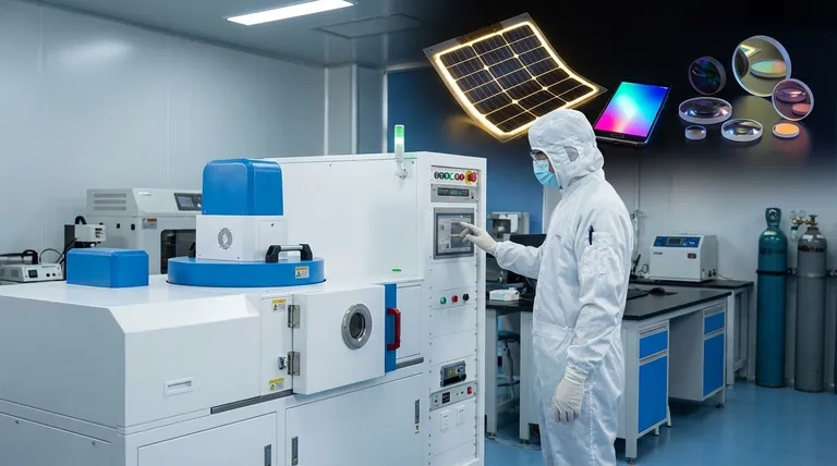
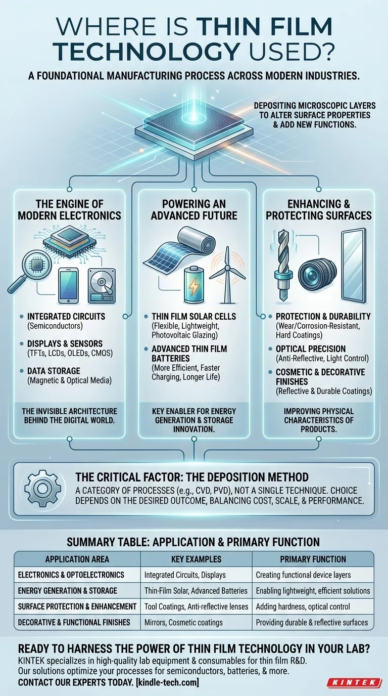
At its core, thin film technology is a foundational manufacturing process used across nearly every modern industry. You encounter its applications in consumer electronics like smartphones and displays, in energy production through solar cells and advanced batteries, and in everyday items requiring protective or reflective coatings, from medical equipment to mirrors.
The crucial insight is that "thin film" is not a single product, but a method of depositing microscopic layers of material onto a surface. This process fundamentally alters the surface's properties, adding functions like electrical conductivity, insulation, hardness, or light reflection where they didn't exist before.
The Engine of Modern Electronics
The most significant impact of thin film technology is in the fabrication of electronic and optoelectronic components. It is the invisible architecture behind the digital world.
In Integrated Circuits (Semiconductors)
The microchips that power all computing are built using thin film deposition. This process creates the incredibly complex, layered structures of conductive, insulating, and semiconducting materials that form transistors and circuits.
In Displays and Sensors
Thin film transistors (TFTs) are essential for modern screens, including liquid crystal displays (LCDs) and OLEDs. These films allow for the precise control of individual pixels, leading to better response times and higher energy efficiency. This same technology is vital for camera sensors (CMOS) and other optical devices.
For Data Storage
Thin film deposition is also used to create the magnetic layers on hard disk drives and the reflective surfaces on CDs and other optical media, enabling high-density information storage.
Powering an Advanced Future
Thin film technology is a key enabler for advancements in energy generation, storage, and efficiency. Its ability to create lightweight and highly efficient functional surfaces is driving innovation.
Thin Film Solar Cells
Unlike traditional silicon panels, thin film solar cells are flexible, lighter, and can be applied to various surfaces. This makes them ideal for applications like photovoltaic glazing on buildings, where windows can simultaneously generate electricity.
Advanced Thin Film Batteries
By using thin films, batteries can be made more efficient, charge significantly faster, and have a longer lifespan. This is critical for improving performance in medical implants, smart cards, and large-scale green energy storage banks.
Enhancing and Protecting Physical Surfaces
Beyond electronics, thin films are used to improve the physical characteristics of a vast range of products, from industrial tools to consumer goods.
For Protection and Durability
Extremely hard, corrosion-resistant, and heat-resistant films can be deposited on surfaces to protect them from wear and oxidation. This extends the life of mechanical components, tools, and medical equipment.
For Optical Precision
Thin films are applied to optical components like lenses and mirrors to control the reflection and transmission of light. Anti-reflective coatings on eyeglasses and camera lenses are a common example.
For Cosmetic and Decorative Finishes
On a simpler level, thin film deposition is used for cosmetic purposes. This includes creating the reflective surfaces of mirrors and toys or applying durable, decorative coatings to a variety of products.
The Critical Factor: The Deposition Method
It is important to understand that "thin film technology" refers to a category of processes, not a single technique. The specific method used to deposit the film is a critical decision.
A Process Tailored to the Goal
The choice of deposition technology—such as chemical vapor deposition (CVD) or physical vapor deposition (PVD)—depends entirely on the desired outcome. There is no one-size-fits-all solution.
Balancing Cost, Scale, and Performance
Different methods offer distinct trade-offs between cost, speed of production, the precision of the film, and the final material properties. The process for creating a simple decorative coating is vastly different and less complex than that required for a semiconductor.
How to Apply This Understanding
The specific application of thin film technology is always dictated by the primary goal for the material's surface.
- If your primary focus is electrical performance: Thin films are used to build the microscopic layers of insulators and conductors that form an integrated circuit.
- If your primary focus is energy innovation: The technology enables lightweight solar cells and more efficient, faster-charging batteries.
- If your primary focus is material durability: It provides super hard, corrosion-resistant coatings to protect surfaces from physical and chemical damage.
- If your primary focus is optical control: The films are engineered to precisely manage light reflection and transmission for lenses, sensors, and displays.
Ultimately, thin film technology is a versatile and essential tool for manipulating matter at a microscopic scale to achieve a specific functional goal.
Summary Table:
| Application Area | Key Examples | Primary Function |
|---|---|---|
| Electronics & Optoelectronics | Integrated Circuits, Displays (TFTs), Sensors | Creating conductive, insulating, and semiconducting layers for devices. |
| Energy Generation & Storage | Thin-Film Solar Cells, Advanced Batteries | Enabling lightweight, flexible energy solutions and faster charging. |
| Surface Protection & Enhancement | Wear-resistant tool coatings, Anti-reflective lenses | Adding hardness, corrosion resistance, and optical control to surfaces. |
| Decorative & Functional Finishes | Mirrors, Cosmetic coatings | Providing durable and reflective surfaces for consumer goods. |
Ready to Harness the Power of Thin Film Technology in Your Lab?
Thin film deposition is a cornerstone of modern material science, enabling breakthroughs in electronics, energy, and surface engineering. The right equipment is critical to achieving your specific performance goals, whether you are developing semiconductors, advanced batteries, or protective coatings.
KINTEK specializes in high-quality lab equipment and consumables for all your thin film research and development needs. We provide the reliable tools and expert support necessary to push the boundaries of innovation.
Contact our experts today to discuss how our solutions can help you optimize your thin film processes and bring your next project to life.
Visual Guide
Related Products
- Vacuum Hot Press Furnace Machine for Lamination and Heating
- Electron Beam Evaporation Coating Oxygen-Free Copper Crucible and Evaporation Boat
- Molybdenum Tungsten Tantalum Evaporation Boat for High Temperature Applications
- Lab Blown Film Extrusion Three Layer Co-Extrusion Film Blowing Machine
- Aluminum-Plastic Flexible Packaging Film for Lithium Battery Packaging
People Also Ask
- What role does the high vacuum environment play in sintering graphite film/aluminum composites? Optimize Your Bonding
- What role does mechanical pressure play during the vacuum diffusion bonding of tungsten and copper? Keys to Solid Bonding
- How does the vacuum system within a vacuum hot press furnace contribute to the quality of aluminum matrix composites?
- What are the advantages of using a vacuum hot press furnace for sintering CNT/Cu composites? Superior Density & Bonding
- What advantages does a vacuum hot press furnace provide for LSLBO ceramic electrolytes? Achieve 94% Relative Density


