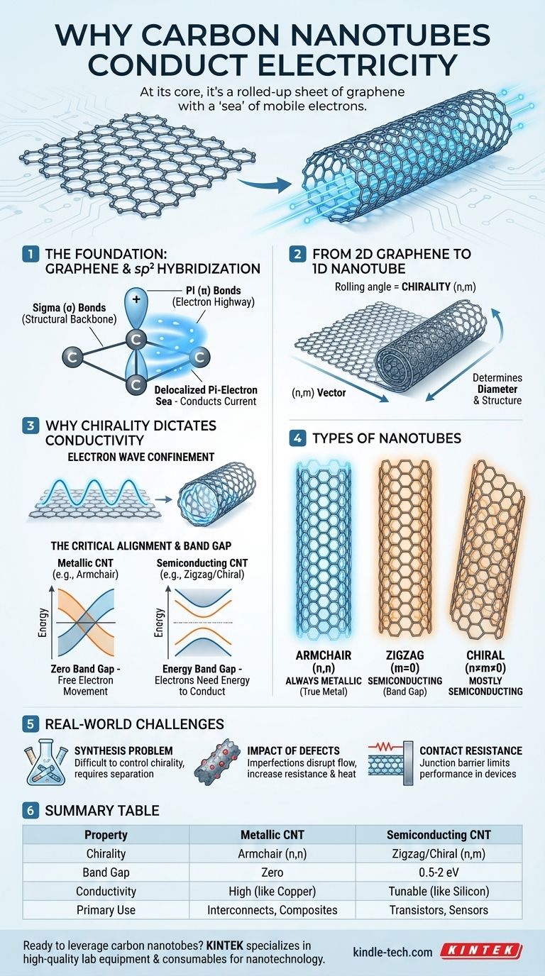
At its core, a carbon nanotube conducts electricity because its structure is a rolled-up sheet of graphene. The carbon atoms are bonded in a way that leaves a "sea" of mobile electrons free to move along the tube's length. However, the exact way the sheet is rolled determines how well it conducts, making some nanotubes metallic like copper and others semiconducting like silicon.
The conductivity of a carbon nanotube is not a fixed property; it is a direct consequence of its geometry. The specific angle at which the graphene sheet is conceptually rolled, known as its chirality, dictates whether the electron energy states align to create a metal or form an energy gap, creating a semiconductor.

The Foundation: Graphene's sp² Hybridization
The Role of Carbon's Orbitals
Carbon atoms in a nanotube are connected using sp² hybridization. This is the same bonding arrangement found in graphite and graphene.
Each carbon atom uses three of its four outer electrons to form strong covalent bonds with its neighbors.
Sigma Bonds: The Structural Backbone
These three electrons create sigma (σ) bonds that lie in the same plane. These bonds form the famously strong hexagonal lattice that gives a nanotube its incredible mechanical strength.
These sigma electrons are localized and tightly bound, forming the structural framework but not contributing to electrical conduction.
Pi Bonds: The Highway for Electrons
The fourth outer electron from each carbon atom resides in a p-orbital perpendicular to the nanotube's surface.
These p-orbitals overlap with those on neighboring atoms, creating delocalized pi (π) bonds. This forms a cloud of electrons that are not tied to any single atom but are free to move across the entire structure. It is this "pi-electron sea" that carries electrical current.
From 2D Graphene to 1D Nanotube
Introducing Chirality
Imagine a flat sheet of graphene. To make a nanotube, you roll this sheet into a seamless cylinder. The angle at which you roll it is called its chirality.
This geometric property is the single most important factor determining the nanotube's electrical behavior.
The Chiral Vector (n,m)
Scientists describe a nanotube's chirality with a pair of indices, (n,m). These integers define the direction and angle of the roll, which in turn determines the nanotube's diameter and structure.
You don't need to know the complex math, only that different (n,m) pairs correspond to different types of nanotubes.
Why Chirality Dictates Conductivity
Electron Wave Confinement
In quantum mechanics, electrons behave like waves. In a flat graphene sheet, these electron waves can travel in any direction.
When the sheet is rolled into a tube, the wave is confined. It can only travel around the circumference in specific, quantized wavelengths that "fit" perfectly. This confinement imposes strict rules on which electron energy states are allowed.
The Critical Alignment
A material is metallic if its electrons can easily jump into a state where they can move freely (a conduction band). It's a semiconductor if there's an energy gap they must overcome first.
For a CNT to be metallic, its allowed electron wave states (due to confinement) must perfectly align with the energy states where conduction occurs in graphene.
Armchair Nanotubes (n,n)
For nanotubes with an "armchair" structure—where n=m (e.g., (10,10))—this alignment always occurs. The geometry guarantees that there is no energy gap.
Therefore, all armchair nanotubes are true metals.
Zigzag and Chiral Nanotubes (n,m)
For all other types, known as "zigzag" (where m=0) and "chiral" (where n≠m≠0), the alignment is a matter of chance.
Based on their geometry, roughly one-third of these nanotubes will be metallic, while the other two-thirds will have their electron states misaligned. This misalignment opens up an energy band gap, making them semiconductors. The size of this gap is inversely proportional to the nanotube's diameter.
Common Pitfalls and Real-World Challenges
The Synthesis Problem
The single greatest challenge in nanotube electronics is control over chirality. Most synthesis methods, like chemical vapor deposition, produce a random mixture of metallic and semiconducting nanotubes.
Separating these types is a difficult and costly process, hindering their widespread adoption in applications that require purity.
The Impact of Defects
Real-world nanotubes are not perfect cylinders. Structural defects, impurities, or sharp bends can disrupt the flow of the pi-electrons.
These imperfections act as scattering sites that increase electrical resistance and generate unwanted heat, degrading performance.
The Contact Resistance Hurdle
Even with a perfect metallic nanotube, getting current into and out of it is a significant engineering problem. The junction between the nanotube and a metal electrode can have a very high contact resistance.
In many nano-devices, this contact resistance, not the nanotube's intrinsic resistance, is the limiting factor for performance.
Applying This to Your Project
Understanding this link between structure and property is key to leveraging nanotubes effectively.
- If your primary focus is bulk conductivity (e.g., in composites or inks): You can often use an unseparated mixture, as the network of metallic tubes will provide enough conductive pathways.
- If your primary focus is nano-electronics (e.g., transistors): You require purely semiconducting nanotubes, making post-synthesis separation or chiral-specific growth methods absolutely essential.
- If your primary focus is high-performance wiring (e.g., on-chip interconnects): You need purely metallic, low-defect nanotubes to minimize resistance and maximize current-carrying capacity.
Ultimately, harnessing the remarkable electrical properties of carbon nanotubes depends entirely on controlling their precise atomic geometry.
Summary Table:
| Property | Metallic CNT | Semiconducting CNT |
|---|---|---|
| Chirality | Armchair (n,n) | Zigzag/Chiral (n,m) |
| Band Gap | Zero | 0.5-2 eV (size depends on diameter) |
| Conductivity | High, like copper | Tunable, like silicon |
| Occurrence | ~33% of synthesized tubes | ~67% of synthesized tubes |
| Primary Use | Interconnects, conductive composites | Transistors, sensors, electronics |
Ready to leverage carbon nanotubes in your research or production? KINTEK specializes in high-quality lab equipment and consumables for nanotechnology applications. Whether you need materials for composite development, semiconductor research, or advanced electronics, our expertise can help you achieve precise results. Contact our specialists today to discuss how we can support your specific project requirements with reliable laboratory solutions.
Visual Guide
Related Products
- Carbon Graphite Boat -Laboratory Tube Furnace with Cover
- Boron Nitride (BN) Ceramic Tube
- Hydrophilic Carbon Paper TGPH060 for Battery Lab Applications
People Also Ask
- What is the temperature range of graphite crucible? Choose the Right Crucible for Your High-Temp Application
- What is the technical value of using graphite crucibles with graphite paper liners? Optimize Zr3(Al1-xSi)C2 Synthesis
- Why is a graphite crucible containing molten bismuth used in LiF–NaF–KF purification? Enhance Melt Purity Efficiently
- What metals can you melt in a graphite crucible? A Guide to Safe & Efficient Melting
- What core conditions do high-temperature graphite tube furnaces provide during the pressureless sintering of Boron Carbide (B4C)?