Lab Materials
High Purity Hafnium (Hf) Sputtering Target / Powder / Wire / Block / Granule
Item Number : LM-HF
Price varies based on specs and customizations
- Chemical Formula
- Hf
- Purity
- 2N5-3N5
- Shape
- discs / wire / block / powder / plates / column targets / step target / custom-made

Shipping:
Contact us to get shipping details Enjoy On-time Dispatch Guarantee.
We offer Hafnium (Hf) materials for laboratory use at competitive prices. Our expertise lies in producing and customizing Hafnium (Hf) materials to meet your specific needs, including various purities, shapes, and sizes.
We provide a diverse range of specifications and sizes for sputtering targets (circular, square, tubular, irregular), coating materials, cylinders, cones, particles, foils, powders, 3D printing powders, nanometer powders, wire rods, ingots, blocks, and more.
Details


About Hafnium (Hf)
Hafnium is a relatively rare element with limited technical uses. Its most common application is as a nuclear control rod due to its ability to absorb neutrons. Hafnium is also used in the production of various alloys including iron, titanium, niobium, and tantalum.
Hafnium-based alloys are replacing polysilicon as the principal gate material in Metal-Oxide-Semiconductor Field Effect Transistors (MOSFETs). This replacement has allowed for the development of MOSFET gates smaller than 10 angstroms. Recent research has focused on developing high-k materials which can function as a dielectric barrier or gate with lower leakage.
Hafnium is available in various forms including metal and compounds with different levels of purity ranging from ACS grade to ultra-high purity. Elemental or metallic forms of hafnium include pellets, rods, wires, and granules for evaporation source material purposes. Hafnium nanomaterials provide ultra-high surface area for nanotechnology research.
Hafnium oxide is available in powder and dense pellet form for various uses such as optical coating and thin film applications. Hafnium is also available in soluble forms including chloride, nitrate, and acetate, and insoluble forms such as fluorides. These compounds can be manufactured as solutions at specified stoichiometries.
Ingredient Quality Control
- Raw material composition analysis
- Through the use of equipment such as ICP and GDMS, the content of metal impurities is detected and analyzed to ensure that it meets the purity standard;
Non-metallic impurities are detected by equipment such as carbon and sulfur analyzers, nitrogen and oxygen analyzers. - Metallographic flaw detection analysis
- The target material is inspected using flaw detection equipment to ensure that there are no defects or shrinkage holes inside the product;
Through metallographic testing, the internal grain structure of the target material is analyzed to ensure that the grains are fine and dense. - Appearance and dimension inspection
- Product dimensions are measured using micrometers and precision calipers to ensure compliance with drawings;
The surface finish and cleanliness of the product are measured using a surface cleanliness meter.
Conventional Sputtering Target Sizes
- Preparation process
- hot isostatic pressing, vacuum melting, etc.
- Sputtering target shape
- plane sputtering target, multi-arc sputtering target, step sputtering target, special-shaped sputtering target
- Round sputtering target size
- Diameter: 25.4mm / 50mm / 50.8mm / 60mm / 76.2mm / 80mm / 100mm / 101.6mm / 152.4mm
Thickness: 3mm / 4mm / 5mm / 6mm / 6.35mm
Size can be customized. - Square sputtering target size
- 50×50×3mm / 100×100×4mm / 300×300×5mm, size can be customized
Available Metal Forms
Metal Forms Details
We manufacture almost all the metals listed on the periodic table in a wide range of forms and purities, as well as standard sizes and dimensions. We can also produce custom-made products to meet specific customer requirements, such as size, shape, surface area, composition, and more. The following list provides a sample of the forms we offer, but it is not exhaustive. If you need laboratory consumables, please contact us directly to request a quote.
- Flat/Planar Forms: Board, Film, Foil, Microfoil, Microleaf, Paper, Plate, Ribbon, Sheet, Strip, Tape, Wafer
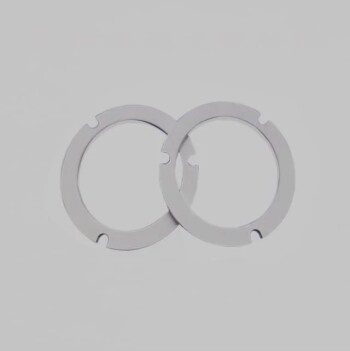
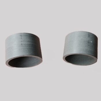
- Preformed Shapes: Anodes, Balls, Bands, Bars, Boats, Bolts, Briquettes, Cathodes, Circles, Coils, Crucibles, Crystals, Cubes, Cups, Cylinders, Discs, Electrodes, Fibers, Filaments, Flanges, Grids, Lenses, Mandrels, Nuts, Parts, Prisms, Pucks, Rings, Rods, Shapes, Shields, Sleeves, Springs, Squares, Sputtering Targets, Sticks, Tubes, Washers, Windows, Wires
- Microsizes: Beads, Bits, Capsules, Chips, Coins, Dust, Flakes, Grains, Granules, Micropowder, Needles, Particles, Pebbles, Pellets, Pins, Pills, Powder, Shavings, Shot, Slugs, Spheres, Tablets
- Macrosizes: Billets, Chunks, Cuttings, Fragments, Ingots, Lumps, Nuggets, Pieces, Punchings, Rocks, Scraps, Segments, Turnings
- Porous and Semi-Porous: Fabric, Foam, Gauze, Honeycomb, Mesh, Sponge, Wool
- Nanoscale: Nanoparticles, Nanopowders, Nanofoils, Nanotubes, Nanorods, Nanoprisms
- Others: Concentrate, Ink, Paste, Precipitate, Residue, Samples, Specimens
KinTek specializes in the manufacturing of high-purity and ultra-high-purity materials with a purity range of 99.999% (5N), 99.9999% (6N), 99.99995% (6N5), and in some cases, up to 99.99999% (7N). Our materials are available in specific grades, including UP/UHP, semiconductor, electronic, deposition, fiber optic, and MBE grades. Our high-purity metals, oxides, and compounds are specifically crafted to meet the rigorous demands of high-technology applications and are ideal for use as dopants and precursor materials for thin film deposition, crystal growth of semiconductors, and synthesis of nanomaterials. These materials find use in advanced microelectronics, solar cells, fuel cells, optical materials, and other cutting-edge applications.
Packaging
We use vacuum packaging for our high-purity materials, and each material has specific packaging tailored to its unique characteristics. For instance, our Hf sputter target is externally tagged and labeled to facilitate efficient identification and quality control. We take great care to prevent any damage that could occur during storage or transportation.
FAQ
What Are High Purity Materials?
What Are High Purity Metals?
What Are High Purity Metals Used For?
What Are The Benefits Of Using High-purity Metals?
Which Industries Commonly Use High-purity Metals?
4.9
out of
5
Absolutely satisfied with the quality of Hafnium Sputtering Target from KINTEK SOLUTION. The purity level is exceptional and meets our research requirements precisely.
4.7
out of
5
KINTEK's Hafnium Powder has been a game-changer for our lab's nanotechnology research. Its ultra-high surface area has opened up new possibilities for our experiments.
4.8
out of
5
The Hafnium Wire from KINTEK SOLUTION arrived promptly and exceeded our expectations. Its consistent quality has ensured reliable results in our thin-film deposition processes.
4.6
out of
5
KINTEK SOLUTION's Hafnium Block has proven to be an excellent choice for our sputtering applications. Its high density and purity have contributed to the success of our research.
4.8
out of
5
We have been thoroughly impressed with the Hafnium Granules from KINTEK SOLUTION. Their uniform size and purity have enabled us to achieve consistent and precise results in our experiments.
4.9
out of
5
KINTEK SOLUTION's Hafnium Sputtering Target has been an outstanding addition to our laboratory. Its durability has ensured long-lasting performance, saving us both time and resources.
4.7
out of
5
The Hafnium Powder from KINTEK SOLUTION has been instrumental in our groundbreaking research. Its exceptional purity and fine particle size have allowed us to explore new frontiers in materials science.
4.8
out of
5
We highly recommend the Hafnium Wire from KINTEK SOLUTION. Its consistent quality and ease of handling have made it an indispensable tool in our laboratory.
4.6
out of
5
KINTEK SOLUTION's Hafnium Block is an excellent choice for high-temperature applications. Its exceptional thermal conductivity has enabled us to achieve outstanding results in our research.
4.8
out of
5
The Hafnium Granules from KINTEK SOLUTION have been a valuable asset to our laboratory. Their uniform size and purity have contributed to the accuracy and reliability of our experiments.
REQUEST A QUOTE
Our professional team will reply to you within one business day. Please feel free to contact us!
Related Products
Hafnium Carbide (HfC) Sputtering Target / Powder / Wire / Block / Granule
Discover our high-quality Hafnium Carbide (HfC) materials tailored to suit your unique laboratory needs. We offer various sizes and specifications of sputtering targets, coating materials, powders, and more. Get reasonable prices and excellent service. Order now.
High Purity Hafnium Oxide (HfO2) Sputtering Target / Powder / Wire / Block / Granule
Get high-quality Hafnium Oxide (HfO2) materials for your laboratory needs at affordable prices. Our customized products come in various sizes and shapes, including sputtering targets, coatings, powders, and more.
High Purity Tungsten (W) Sputtering Target / Powder / Wire / Block / Granule
Find high-quality Tungsten (W) materials for your laboratory needs at affordable prices. We offer customized purities, shapes, and sizes of sputtering targets, coating materials, powders, and more.
High Purity Zirconium (Zr) Sputtering Target / Powder / Wire / Block / Granule
Looking for high-quality Zirconium materials for your laboratory needs? Our range of affordable products includes sputtering targets, coatings, powders, and more, tailored to your unique requirements. Contact us today!
High Purity Zinc (Zn) Sputtering Target / Powder / Wire / Block / Granule
Find high-quality Zinc (Zn) materials for laboratory use at affordable prices. Our experts produce and customize materials of different purities, shapes, and sizes to suit your needs. Browse our range of sputtering targets, coating materials, and more.
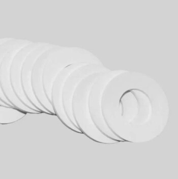
Hexagonal Boron Nitride (HBN) Spacer - Cam Profile and Various Spacer Types
Hexagonal boron nitride (HBN) gaskets are made from hot-pressed boron nitride blanks. Mechanical properties similar to graphite, but with excellent electrical resistance.

High Purity Niobium (Nb) Sputtering Target / Powder / Wire / Block / Granule
Looking for customized Niobium materials for laboratory use? Our experts offer tailored solutions with different purities, shapes, and sizes at reasonable prices. Discover our wide range of Niobium products.
High Purity Tantalum (Ta) Sputtering Target / Powder / Wire / Block / Granule
Discover our high-quality Tantalum (Ta) materials for laboratory use at affordable prices. We tailor to your specific requirements with various shapes, sizes, and purities. Explore our range of sputtering targets, coating materials, powders, and more.
Hexagonal Boron Nitride (HBN) Ceramic Ring
Boron nitride ceramic (BN) rings are commonly used in high temperature applications such as furnace fixtures, heat exchangers and semiconductor processing.
High Purity Titanium (Ti) Sputtering Target / Powder / Wire / Block / Granule
Shop for high-quality Titanium (Ti) materials at reasonable prices for laboratory use. Find a wide range of tailored products to suit your unique needs, including sputtering targets, coatings, powders, and more.
Boron Nitride (BN) Ceramics-Conductive Composite
Due to the characteristics of boron nitride itself, the dielectric constant and dielectric loss are very small, so it is an ideal electrical insulating material.
Boron Nitride (BN) Ceramic Parts
Boron nitride ((BN) is a compound with high melting point, high hardness, high thermal conductivity and high electrical resistivity. Its crystal structure is similar to graphene and harder than diamond.
High Purity Aluminum (Al) Sputtering Target / Powder / Wire / Block / Granule
Get high-quality Aluminum (Al) materials for laboratory use at affordable prices. We offer customized solutions including sputtering targets, powders, foils, ingots & more to meet your unique needs. Order now!
High Purity Germanium (Ge) Sputtering Target / Powder / Wire / Block / Granule
Get high-quality gold materials for your laboratory needs at affordable prices. Our custom-made gold materials come in various shapes, sizes, and purities to fit your unique requirements. Explore our range of sputtering targets, coating materials, foils, powders, and more.
Boron Nitride (BN) Ceramic Rod
Boron nitride (BN) rod is the strongest boron nitride crystal form like graphite, which has excellent electrical insulation, chemical stability and dielectric properties.
High Purity Lead (Pb) Sputtering Target / Powder / Wire / Block / Granule
Looking for high-quality Lead (Pb) materials for your laboratory needs? Look no further than our specialized selection of customizable options, including sputtering targets, coating materials, and more. Contact us today for competitive pricing!

Silicon Nitride (SiN) Ceramic Sheet Precision Machining Ceramic
Silicon nitride plate is a commonly used ceramic material in the metallurgical industry due to its uniform performance at high temperatures.
Aluminum Nitride (AlN) Sputtering Target / Powder / Wire / Block / Granule
High-quality Aluminum Nitride (AlN) materials in various shapes and sizes for laboratory use at affordable prices. Explore our range of sputtering targets, coatings, powders, and more. Customized solutions available.
High Purity Rhodium (Rh) Sputtering Target / Powder / Wire / Block / Granule
Get high-quality Rhodium materials for your lab needs at great prices. Our expert team produces and customizes Rhodium of various purities, shapes, and sizes to fit your unique requirements. Choose from a wide range of products, including sputtering targets, coating materials, powders, and more.

Boron Nitride (BN) Ceramic Plate
Boron nitride (BN) ceramic plates do not use aluminum water to wet, and can provide comprehensive protection for the surface of materials that directly contact molten aluminum, magnesium, zinc alloys and their slag.
Boron Nitride (BN) Ceramic Tube
Boron nitride (BN) is known for its high thermal stability, excellent electrical insulating properties and lubricating properties.
Related Articles

Cold Isostatic Pressing vs. Hot Isostatic Pressing Which is Better
Isostatic pressing is a process used in the production of high-performance materials and components. It involves applying uniform pressure on all sides of a material or part, resulting in a more uniform density and improved mechanical properties.
PVD Sputtering Targets and Hot Isostatic Pressing: Part 2
This article discusses the manufacturing and optimization of PVD sputtering targets, focusing on techniques like hot isostatic pressing and high pressure heat treatment.
PVD Sputtering Targets and Hot Isostatic Pressing: Part 1
Explores the use of hot isostatic pressing in producing high-quality sputtering targets and the applications of PVD sputtering technology.
Hot Isostatic Pressing: A Versatile Technology for Advanced Material Processing
Explores the origins, principles, and applications of hot isostatic pressing in various material fields.