Introduction to PECVD Coatings in Solar Cell Manufacturing
Importance of PECVD in Solar Cell Quality
PECVD (Plasma-Enhanced Chemical Vapor Deposition) coating plays a pivotal role in enhancing both the performance and aesthetic appeal of crystalline silicon solar cells. This process is instrumental in determining the market acceptance and cost-efficiency of solar cells, making it a critical component in the solar energy industry.
Key Benefits of PECVD Coating
-
Enhanced Light Absorption: The silicon nitride film formed through PECVD can significantly reduce light reflection, thereby increasing the amount of light absorbed by the solar cell. This improvement directly translates to higher energy conversion efficiency.
-
Improved Surface Passivation: The hydrogen present in the silicon nitride film passivates the surface of the solar cell, reducing the surface recombination rate of the emitting junction. This reduction in dark current leads to an increase in the open circuit voltage, further boosting the overall photoelectric conversion efficiency.
-
Uniform Coating: PECVD's versatility allows for the even application of coatings on relatively wide surface areas, such as solar panels and optical glass. The refractive quality of these coatings can be finely tuned by adjusting the plasma, offering an extremely high degree of process control.

Application in Solar Cell Manufacturing
The PECVD process involves several intricate steps:
- Initial Setup: The silicon wafer is placed on the lower electrode, with the space between the graphite boats serving as the reaction zone.
- Reaction Initiation: Reactants (SiH4 + NH3) are injected into the reaction furnace, followed by electric field decomposition.
- Molecular Diffusion: Primary molecules diffuse and adsorb, while secondary molecules disperse into the silicon wafer.
- Surface Reaction: A continuous film forms through surface reactions, ultimately yielding a silicon nitride film.
This detailed process ensures that the solar cells not only function optimally but also meet stringent aesthetic standards, crucial for market acceptance.
Broader Applications
Beyond solar cells, PECVD technology finds applications in various fields:
- Optical Devices: Used in the production of sunglasses, tinted optical devices, and photometers.
- Food Packaging: Employed to create dense, inert coatings for packaging materials like potato chip bags.
- Biomedical Implants: Utilized for producing high-purity coatings on medical implants.
These diverse applications underscore the versatility and importance of PECVD in modern technology and industry.
Challenges in PECVD Process
The complexity of the PECVD process leads to various rework issues, necessitating detailed analysis and targeted solutions. Several factors contribute to these challenges, including equipment malfunctions, process parameter variations, and environmental conditions.
Equipment Malfunctions
- Gas Flow Meter Issues: Regular checks are essential to ensure the gas flow meter operates normally, as anomalies can disrupt the gas supply and affect film deposition uniformity.
- Vacuum Pump Abnormalities: The vacuum pump's performance is critical. Using a vacuum gauge to measure the pumping speed can help identify and rectify any issues promptly.
- RF Matching Circuit Faults: Faults in the RF matching circuit can lead to poor film quality. Monitoring the reflected power of the RF source and checking the capacitor and inductor in the matching circuit are necessary steps.
Process Parameter Variations
- Plate Spacing and Reaction Chamber Size: Optimal plate spacing is crucial. A larger spacing reduces substrate damage but can exacerbate the edge effect of the electric field, affecting deposition uniformity. The reaction chamber size, while increasing productivity, can also impact thickness uniformity.
- RF Power and Frequency: Higher RF power enhances film quality but increases substrate damage. The frequency of the RF power supply significantly affects film uniformity, with high frequencies producing more uniform films compared to low frequencies.
- Air Pressure: The air pressure during plasma formation influences the deposition rate and film quality. High pressure increases the deposition rate but can reduce film density and increase defects, while low pressure affects the film's deposition mechanism.
Environmental Conditions
- Substrate Temperature: The substrate temperature significantly impacts film quality, affecting local state density, electron mobility, and optical properties. Higher temperatures result in denser films but have minimal impact on the deposition rate.
- Chamber Cleanliness: Maintaining the cleanliness of the process chamber is vital. Contaminants can lead to poor film quality and defects. Regular cleaning and monitoring are necessary to ensure optimal conditions.
These challenges highlight the intricate balance required in the PECVD process. Addressing these issues through meticulous analysis and precise adjustments can significantly enhance the quality and efficiency of PECVD coatings.
Common Causes of PECVD Rework and Their Solutions
Edge Color Difference
The phenomenon of edge color difference in PECVD coatings is primarily attributed to discrepancies in the spacing between sheets within the graphite boat. This uneven spacing results in non-uniform electric fields and inconsistent coating rates across the solar cell surface. The variations in electric fields can lead to localized areas of over-coating or under-coating, which manifest as visible color differences at the edges of the coated cells.
To mitigate this issue, several corrective measures can be implemented. Firstly, regular inspections of the ceramic spacers and rods are essential. These components play a critical role in maintaining consistent spacing within the graphite boat. Any signs of wear or damage should be promptly addressed by replacing the affected parts. Additionally, ensuring that the ceramic spacers and rods are properly aligned can help in maintaining a uniform electric field distribution.
Moreover, the process of checking and replacing these components should be part of a routine maintenance schedule. By adhering to a structured maintenance plan, manufacturers can prevent the recurrence of edge color differences and ensure a more consistent coating quality. This proactive approach not only enhances the visual appeal of the solar cells but also improves their overall performance and market acceptance.
In summary, addressing edge color difference in PECVD coatings involves meticulous attention to the graphite boat's spacing mechanisms. By regularly checking and replacing ceramic spacers and rods, manufacturers can achieve a more uniform electric field and coating rate, thereby minimizing color variations and improving the quality of the final product.
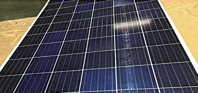
Center Color Difference
The phenomenon of center color difference in PECVD coatings primarily stems from two critical factors: inadequate gas flow and improper positioning of the substrate. When the gas flow is insufficient, the reactive gases fail to distribute uniformly across the surface of the substrate, leading to thinner film deposition in the central region. Similarly, improper positioning can misalign the substrate within the reactor, resulting in non-uniform exposure to the plasma and subsequent variations in film thickness.
To mitigate this issue, several targeted solutions are employed. Firstly, ensuring the cleanliness and unobstructed flow of air inlet holes is paramount. Accumulated debris or blockages in these holes can significantly impede gas flow, necessitating regular cleaning and maintenance. Additionally, the positioning points of the substrate must be meticulously inspected and repaired. Any misalignment or wear in these points can cause the substrate to sit unevenly, exacerbating the center color difference.
In summary, addressing center color difference involves a dual approach: optimizing gas flow dynamics and ensuring precise substrate positioning. By implementing these corrective measures, manufacturers can enhance the uniformity and quality of PECVD coatings, thereby improving the overall performance of crystalline silicon solar cells.
Scratches
Scratches in PECVD coatings are frequently the result of manual handling errors or wear at critical positioning points, such as those found on graphite boats. These issues can arise during the delicate process of wafer handling, where even minor deviations can lead to significant surface damage. The presence of scratches not only compromises the aesthetic appeal of the solar cells but also affects their overall performance and marketability.
To mitigate these issues, several corrective measures can be implemented:
-
Adjustment of Suction Pen Power: Fine-tuning the suction pen power can help in maintaining a more controlled and gentle handling of the wafers, reducing the likelihood of scratches. This adjustment ensures that the wafers are neither too loosely nor too tightly held, thereby minimizing surface contact and potential damage.
-
Repair and Maintenance of Graphite Boat Points: Regular inspection and repair of graphite boat points are essential. Wear and tear at these points can lead to uneven handling and increased friction, causing scratches. By ensuring that these points are in optimal condition, the risk of scratches can be significantly reduced.
-
Implementation of Automated Handling Systems: Introducing automated handling systems can further minimize the risk of scratches. These systems can provide more precise and consistent handling compared to manual processes, thereby reducing the human error factor.
By addressing these areas, manufacturers can effectively reduce the incidence of scratches in PECVD coatings, thereby improving the quality and reliability of crystalline silicon solar cells.
Silicon Removal
Silicon removal is a common issue in the PECVD coating process for crystalline silicon solar cells, primarily caused by collisions during the lowering of wafers into the PECVD furnace. These collisions can result in significant damage to the wafers, necessitating rework and increasing production costs.
To mitigate this issue, several preventive measures can be implemented:
-
Cleaning Suction Pens: Regularly cleaning the suction pens ensures that they operate efficiently, reducing the likelihood of wafer collisions during lowering. This involves using appropriate cleaning agents and techniques to remove any debris or residue that could interfere with the suction process.
-
Checking Graphite Boat Points: Inspecting and maintaining the graphite boat points is crucial. Any wear or damage to these points can lead to misalignment during wafer lowering, causing collisions. Regular checks and timely repairs or replacements can prevent such issues.
-
Optimizing Lowering Mechanisms: Enhancing the mechanisms responsible for lowering the wafers can also help. This includes fine-tuning the lowering speed and ensuring precise control over the lowering process to minimize the risk of collisions.
By addressing these areas, manufacturers can significantly reduce the incidence of silicon removal, thereby improving the overall quality and efficiency of the PECVD coating process.
Abnormal Discharge
Abnormal discharge in the PECVD (Plasma-Enhanced Chemical Vapor Deposition) process is a significant issue that can arise due to the accumulation of debris on the electrodes or at the bottom of the PECVD furnace. This debris, often a byproduct of the coating process, can interfere with the normal operation of the electrodes, leading to irregular discharges and potentially damaging the quality of the coating on the solar cells.
To mitigate this issue, a comprehensive approach involving both pre-feeding checks and regular maintenance is essential. Pre-feeding checks ensure that the electrodes and the furnace interior are free from any debris or contaminants before the process begins. This involves a thorough inspection and cleaning regimen that can prevent the initial buildup of debris.
Regular maintenance is equally crucial. It includes scheduled cleanings of the electrodes and the furnace bottom, as well as periodic checks to ensure that all components are functioning optimally. By adhering to a strict maintenance schedule, manufacturers can significantly reduce the likelihood of abnormal discharges, thereby maintaining the consistency and quality of the PECVD coatings.
Implementing these preventive measures not only enhances the efficiency of the PECVD process but also extends the lifespan of the equipment, reducing the overall costs associated with frequent rework and repairs.
Conclusion and Future Prospects
Impact of PECVD Quality on Solar Cell Industry
Improving the quality of the Plasma-Enhanced Chemical Vapor Deposition (PECVD) process can lead to substantial advancements in solar cell performance and manufacturing efficiency. PECVD is a pivotal technology in the production of solar cells, enabling the deposition of thin films that enhance light absorption and reduce reflection, thereby boosting the overall efficiency of photovoltaic devices.
The versatility of PECVD allows for precise control over the deposition process, which is crucial for achieving high-quality coatings on large surface areas such as solar panels. By fine-tuning the plasma conditions, manufacturers can achieve uniform coatings with optimal optical properties, which are essential for maximizing the energy conversion efficiency of solar cells.
Moreover, the ability to produce dense, inert coatings with high purity makes PECVD indispensable not only in the solar industry but also in various other sectors, including biomedical applications and food packaging. In the context of solar cells, the silicon nitride film formed through PECVD plays a dual role: it not only reduces light reflection but also passivates the solar cell surface, thereby reducing the surface recombination rate and enhancing the open circuit voltage.
The benefits of enhanced PECVD quality extend beyond just improving solar cell performance. By enabling more efficient manufacturing processes, higher quality PECVD coatings can significantly reduce production costs, making solar energy more competitive in the global energy market. This, in turn, contributes to the broader goal of sustainable energy solutions, helping to address environmental challenges and promote a cleaner, more sustainable future.
Role of PECVD in Sustainable Energy Solutions
The role of Plasma-Enhanced Chemical Vapor Deposition (PECVD) in sustainable energy solutions is multifaceted and increasingly pivotal. PECVD processes are not only integral to the semiconductor industry but also play a crucial role in advancing solar energy technologies. By enabling the deposition of thin films with high uniformity and precision, PECVD optimizes the efficiency of solar cells, thereby enhancing their energy conversion rates.
In the realm of solar cells and photovoltaics, PECVD's versatility shines through its ability to apply uniform coatings over extensive surface areas, such as solar panels and optical glass. This capability allows for fine-tuning of the optical properties of these surfaces, which is essential for maximizing light absorption and conversion efficiency. The refractive quality of the optical layer can be meticulously adjusted by modifying the plasma parameters, resulting in highly controlled and efficient processes.
Moreover, PECVD systems offer significant advantages such as low-temperature processing and high throughput, which are critical for maintaining the integrity of sensitive materials used in solar cells. These attributes ensure that the solar cells produced are not only efficient but also durable and cost-effective, aligning perfectly with the goals of sustainable energy solutions.
The integration of PECVD technology in solar cell manufacturing signifies a step forward in addressing global energy challenges. By contributing to more efficient solar energy conversion, PECVD processes not only promote sustainability but also pave the way for a greener, more energy-independent future. As the demand for advanced electronic devices and sustainable energy sources continues to grow, the importance of PECVD in the semiconductor and solar industries is set to expand, further solidifying its role in sustainable energy solutions.
Related Products
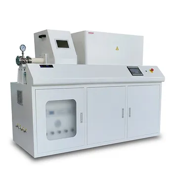
- Inclined Rotary Plasma Enhanced Chemical Vapor Deposition PECVD Equipment Tube Furnace Machine
- Inclined Rotary Plasma Enhanced Chemical Vapor Deposition PECVD Equipment Tube Furnace Machine
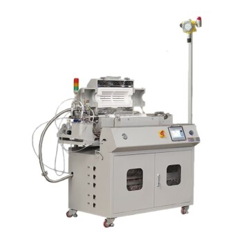
- Chemical Vapor Deposition CVD Equipment System Chamber Slide PECVD Tube Furnace with Liquid Gasifier PECVD Machine
- RF PECVD System Radio Frequency Plasma-Enhanced Chemical Vapor Deposition RF PECVD
- Custom CVD Diamond Coating for Lab Applications

