Introduction to CVD and its Importance
Chemical vapor deposition (CVD) is a crucial process in the semiconductor industry. It involves depositing a thin layer of material onto a substrate by exposing it to a gas-phase precursor. CVD has become a vital technology in the production of electronic devices, including integrated circuits, transistors, and solar panels. The process allows for the deposition of high-quality films with tailored properties, such as thickness, composition, and structure. CVD films have excellent adhesion properties, uniformity, and purity, making them ideal for semiconductor manufacturing. CVD has revolutionized the semiconductor industry, enabling the production of high-performance electronic devices with enhanced functionality and reliability.
Table of Contents
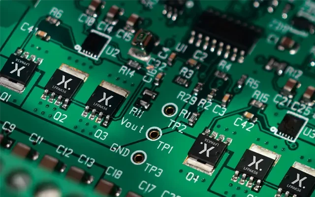
CVD Process in the Semiconductor Industry
Chemical Vapor Deposition (CVD) is an important technique in the semiconductor industry for producing high-quality thin films of various materials such as silicon, silicon dioxide, silicon nitride, and metal films on the semiconductor substrate. The process involves the deposition of a thin layer of material onto a substrate under controlled conditions of temperature, pressure, and gas composition.
CVD Process Steps
The CVD process in the semiconductor industry involves several steps:
-
Preparation of the substrate: The substrate is cleaned and prepared before the deposition process to ensure that it is free from any contaminants that can interfere with the deposition process.
-
Loading the substrate: The substrate is loaded into the CVD chamber, which is then sealed and pumped down to a vacuum.
-
Introduction of precursor gases: The precursor gases are introduced into the chamber. These gases react or decompose on the substrate surface to produce the desired thin film deposit. The gases are typically introduced into the chamber through a gas inlet system.
-
Deposition: The precursor gases react or decompose on the substrate surface to produce the desired thin film deposit. The deposition process is controlled by the temperature, pressure, and gas composition in the chamber.
-
Purging: The chamber is purged with an inert gas, such as nitrogen or argon, to remove any unreacted precursor gases.
-
Unloading the substrate: The substrate is unloaded from the chamber once the deposition process is complete.
Types of CVD Processes
There are several types of CVD processes used in the semiconductor industry, including:
- Atmospheric pressure CVD (APCVD): CVD at atmospheric pressure.
- Low-pressure CVD (LPCVD): CVD under subatmospheric pressure.
- Ultrahigh vacuum CVD (UHVCVD): low-pressure CVD, usually operates at 10−6 Pa (≈10−8 torr).
- Plasma-enhanced CVD (PECVD): CVD using plasma to enhance the deposition process.
- Atomic layer CVD (ALCVD): CVD process that deposits one or a few layers of atoms at a time.
- Hot filament CVD (HFCVD): CVD in which the chamber is heated by an external power source and the substrate is heated by radiation from the heated chamber walls.
- Cold wall CVD (CWCVD): CVD in which only the substrate is directly heated either through induction or by transmitting current through the substrate surface itself or a heater in contact with the substrate.
Advantages of CVD Process
The CVD process has several advantages in the semiconductor industry, including:
-
Uniformity: CVD can produce uniform and conformal films over large areas, which is essential for the fabrication of advanced microelectronic devices.
-
Precision: CVD enables the production of high-quality thin films with precise control over thickness, composition, and structure.
-
Versatility: CVD is a versatile process capable of synthesizing coatings, powders, fibers, nanotubes, and monolithic components.
-
Automation: The CVD process is highly automated and can be used to deposit films with thicknesses ranging from a few nanometers to several microns.
In conclusion, the CVD process plays a crucial role in the semiconductor industry for producing high-quality thin films of various materials. The process is highly automated and can be used to deposit films with precise control over thickness, composition, and structure.
Types of Films Produced by CVD
Chemical Vapor Deposition (CVD) is a versatile technique used to fabricate a wide range of coatings and films with unique properties. These films are produced through the chemical reaction of gaseous precursors on a surface. Here are some of the most common types of films produced by CVD:
Silicon Dioxide (SiO2)
SiO2 is a common dielectric material used in microelectronics. It is produced by reacting silane (SiH4) with oxygen (O2) in the presence of a catalyst such as platinum (Pt) or tungsten (W). SiO2 films produced by CVD are highly uniform and have excellent insulating properties.
Silicon Nitride (Si3N4)
Si3N4 is used as a barrier layer in integrated circuits to prevent the diffusion of impurities. It is produced by reacting silane with ammonia (NH3) in the presence of a catalyst such as tungsten. Si3N4 films produced by CVD have excellent mechanical properties and are highly resistant to wear and tear.
Tungsten (W)
Tungsten films are used as conductive layers in microelectronics. They are highly resistant to corrosion and oxidation, making them ideal for use in harsh environments. Tungsten films are produced by reacting tungsten hexafluoride (WF6) with hydrogen (H2) in the presence of a catalyst such as tungsten.
Diamond Films
Diamond films produced by CVD are widely used in cutting tools, as they have excellent wear resistance and can withstand high temperatures. They are produced by reacting methane (CH4) with hydrogen in the presence of a catalyst such as nickel (Ni) or cobalt (Co).
Carbon Nanotubes
Carbon nanotubes are produced by CVD by reacting a carbon-containing gas such as acetylene (C2H2) or ethylene (C2H4) with a catalyst such as iron (Fe) or cobalt (Co). Carbon nanotubes produced by CVD have unique mechanical and electrical properties, making them useful in a wide range of applications.
Graphene
Graphene is one of the most widely known products of CVD. It is a two-dimensional material that is only made of carbon. Graphene films produced by CVD are highly uniform and have excellent electrical and thermal conductivity. They are produced by reacting a carbon-containing gas such as methane with hydrogen in the presence of a catalyst such as copper (Cu) or nickel (Ni).
In conclusion, CVD is a powerful technique that can be used to produce a wide range of films and coatings with unique properties. These films are produced through the chemical reaction of gaseous precursors on a surface. The types of films that can be produced by CVD are numerous, including SiO2, Si3N4, tungsten, diamond films, carbon nanotubes, and graphene. Each of these films has unique properties that make them useful in a wide range of applications.
Benefits of CVD in the Semiconductor Industry
High-Quality, Uniform Films
Chemical Vapor Deposition (CVD) is widely used in the semiconductor industry to create high-quality, uniform films with excellent control over thickness and composition. This is crucial for ensuring the reliability and performance of semiconductor devices. With CVD technology, it is possible to deposit thin films of materials such as silicon or metal nitrides with high precision, resulting in uniform and flawless films.
Complex Structures and Patterns
Another advantage of CVD technology is its ability to create complex structures and patterns that are difficult to achieve using other techniques. This is because CVD is a highly flexible technology that can be used to produce a wide range of semiconductor components, including transistors, diodes, and microprocessors. The ability to create complex structures and patterns allows semiconductor manufacturers to produce smaller and more powerful devices.
Scalability
CVD technology is highly scalable, making it suitable for high-volume manufacturing processes. This is because CVD can be used to deposit thin films of materials on a large number of substrates simultaneously. This makes CVD technology ideal for mass production of semiconductor devices.
Improved Performance
CVD technology has significantly contributed to the advancement of the semiconductor industry, enabling the development of smaller and more powerful electronic devices. The use of CVD technology has led to improved performance and reliability of semiconductor devices, making them more efficient and cost-effective.
Versatility
CVD technology is highly versatile and can be used to produce a wide range of semiconductor components, including transistors, diodes, and microprocessors. This versatility allows semiconductor manufacturers to produce customized components that meet the specific needs of their customers.
In conclusion, the use of CVD technology has significantly contributed to the advancement of the semiconductor industry. The ability to produce high-quality, uniform films with excellent control over thickness and composition, create complex structures and patterns, scalability, versatility, and improved performance has made CVD technology a critical tool for semiconductor manufacturers.
CVD and Strain Engineering
Chemical Vapor Deposition (CVD) is a versatile technique used in the semiconductor industry to deposit thin films of materials onto a substrate. One of the key applications of CVD in the semiconductor industry is in strain engineering.
What is Strain Engineering?
Strain engineering is the process of intentionally introducing strain into the crystal lattice of semiconductor materials to improve their performance. This is achieved by depositing a thin film of a different material onto the substrate, which causes a strain in the lattice. By carefully controlling the strain, the properties of the semiconductor material can be tuned to improve its electrical and mechanical properties.
CVD and Strain Engineering
CVD is an ideal technique for strain engineering because it allows for the precise control of film thickness and composition, as well as the ability to deposit films onto complex 3D structures. CVD can be used to deposit a wide range of materials, including metals, oxides, and nitrides, which can all be used to produce strain in semiconductor materials.
How CVD is used in Strain Engineering?
In the semiconductor industry, CVD is used to grow films of a variety of materials, such as silicon, silicon dioxide, and metals like tungsten and copper. This process allows for the precise control of film thickness and composition, making it a critical step in the manufacture of advanced semiconductor devices.
Advantages of CVD in Strain Engineering
CVD is particularly useful for strain engineering because it allows for the precise control of film thickness and composition, as well as the ability to deposit films onto complex 3D structures. Additionally, CVD can be used to deposit films at low temperatures, which is critical for the integration of strain engineering into the manufacturing process of advanced semiconductor devices.
Conclusion
In conclusion, CVD is a critical process in the semiconductor industry, used extensively in the production of microelectronics. CVD is particularly useful for strain engineering, a process that can improve the performance of semiconductor materials by introducing strain into their crystal lattice. The ability to deposit films with precise control of thickness and composition makes CVD an ideal technique for strain engineering, allowing for the production of advanced semiconductor devices with improved electrical and mechanical properties.
CVD's Role in the Production of Solar Panels and Integrated Circuits
Chemical Vapor Deposition (CVD) is a widely used technique in the semiconductor industry for the production of solar panels and integrated circuits. In the production of solar panels, CVD is used to deposit thin films of silicon onto a substrate. This process is known as the Chemical Vapor Deposition of Silicon (CVD-Si), and it is used to create the photovoltaic cells that convert sunlight into electricity.
Chemical Vapor Deposition of Silicon (CVD-Si)
CVD-Si is a critical step in the production of solar panels, as it determines the efficiency and durability of the cells. By using CVD, manufacturers can create thin, uniform layers of silicon that are highly efficient at converting sunlight into electricity. The process involves introducing a reactive gas into a reaction chamber, where it reacts with a precursor gas to form a solid film of silicon. This film is then deposited onto a substrate to form the photovoltaic cells.
Chemical Vapor Deposition of Thin Films (CVD-TF)
In the production of integrated circuits, CVD is used to deposit thin films of various materials onto a substrate. This process is known as the Chemical Vapor Deposition of Thin Films (CVD-TF), and it is used to create the various layers and structures that make up an integrated circuit. CVD-TF is a critical step in the production of integrated circuits, as it determines the performance and reliability of the final product.
Application of CVD in Integrated Circuits
CVD is used to create thin films of various materials, such as silicon, carbon, and metal oxides, that are used in the production of integrated circuits. By using CVD, manufacturers can create thin, uniform layers of various materials that are essential for the functionality of the integrated circuit. The process involves introducing a reactive gas into a reaction chamber, where it reacts with a precursor gas to form a solid film of the required material. This film is then deposited onto a substrate to create the various layers and structures that make up the integrated circuit.
Importance of CVD in Semiconductor Industry
In conclusion, CVD is a critical technique in the semiconductor industry for the production of solar panels and integrated circuits. By using CVD, manufacturers can create thin, uniform layers of various materials that are highly efficient and reliable. As the demand for renewable energy and advanced electronics continues to grow, the use of CVD is likely to become even more important in the years to come. Therefore, the semiconductor industry must continue to invest in CVD technology to stay competitive in the market.
Conclusion
In conclusion, CVD has become an essential technique in the semiconductor industry due to its ability to deposit thin films with precise control over their composition and thickness. The process has a wide range of applications, including the production of integrated circuits and solar panels. CVD has helped in strain engineering, where materials are grown with different lattice constants to create strain, which modifies the electronic properties of the material. It also offers the ability to deposit films at low temperatures, making it an ideal process for sensitive materials. The benefits of CVD in the semiconductor industry are immense, and it will continue to play a crucial role in the advancement of electronic devices.
Related Products
- CVD Diamond Dressing Tools for Precision Applications
- Multi Heating Zones CVD Tube Furnace Machine Chemical Vapor Deposition Chamber System Equipment
- CVD Diamond Domes for Industrial and Scientific Applications
- CVD Diamond for Thermal Management Applications
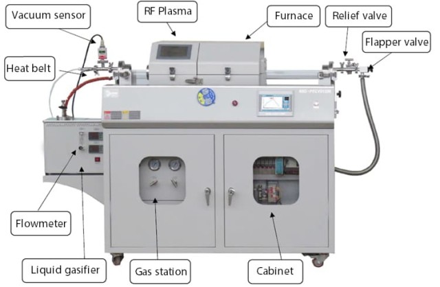
- Chemical Vapor Deposition CVD Equipment System Chamber Slide PECVD Tube Furnace with Liquid Gasifier PECVD Machine


