Introduction to Graphene and Its Preparation Methods
Historical Background and Discovery of Graphene
The study of carbon nanomaterials has long been a focal point in the scientific community, particularly following the discovery of fullerenes and carbon nanotubes. Among these materials, graphene stands out as a unique and intriguing two-dimensional isomer. Initially, graphene was considered thermodynamically unstable due to its planar structure, which defied conventional wisdom about the limitations of carbon's bonding capabilities.
However, in 2004, a groundbreaking experiment at the University of Manchester challenged this assumption. Scientists Andre Geim and Konstantin Novoselov successfully isolated high-quality graphene by exfoliating flakes from highly oriented pyrolytic graphite (HOPG) using adhesive tape. This simple yet ingenious method, known as the "Scotch tape technique," demonstrated that graphene could not only exist but also be produced in a stable and high-quality form.
This discovery marked a pivotal moment in the field of materials science, earning Geim and Novoselov the Nobel Prize in Physics in 2010. Their work not only validated the existence of graphene but also opened new avenues for research and application, sparking a surge of interest in the development of advanced carbon-based materials.
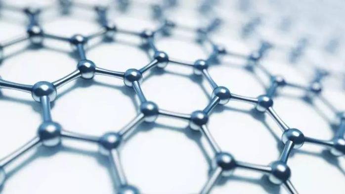
Overview of Graphene Preparation Techniques
Several methods for preparing graphene are available, each with distinct advantages and limitations concerning product quality, yield, and scalability. These methods include tape exfoliation, chemical exfoliation, SiC epitaxial growth, and Chemical Vapor Deposition (CVD).
-
Tape Exfoliation: This method involves physically peeling layers of graphene from bulk graphite using adhesive tape, a technique that was instrumental in the initial discovery of graphene. However, it is limited by its low yield and inability to produce large quantities.
-
Chemical Exfoliation: This process involves the use of solvents and energy to separate graphene layers from graphite. While it can produce high-quality graphene, the yield is typically low, requiring subsequent centrifugation to isolate monolayer and few-layer graphene flakes.
-
SiC Epitaxial Growth: This method relies on the thermal decomposition of silicon carbide (SiC) substrates in ultrahigh vacuum conditions. Although it can produce high-quality graphene, it is constrained by high costs and the need for significant amounts of SiC, making large-scale production challenging.
-
Chemical Vapor Deposition (CVD): CVD is regarded as the most efficient and scalable method for producing large-area graphene. It involves the decomposition of hydrocarbon gases on metal substrates, such as copper or nickel, to form graphene layers. Copper is particularly favored as a substrate due to its ability to support the exclusive deposition of monolayer graphene. Transition metals like cobalt, nickel, and copper have been extensively studied for their suitability in CVD processes, though other metals have yet to match their efficiency in terms of cost, quality, and transferability.
Each of these methods contributes uniquely to the graphene preparation landscape, offering a spectrum of solutions tailored to different applications and production scales.
Chemical Vapor Deposition (CVD) for Graphene Preparation
Principles and Mechanisms of CVD
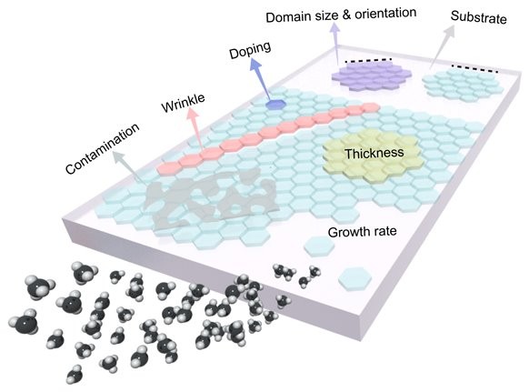
Chemical Vapor Deposition (CVD) is a sophisticated technique that involves the high-temperature decomposition of carbon-containing compounds to grow graphene on various substrates. This process is pivotal in the synthesis of high-quality graphene, which is essential for its myriad applications across different fields. The CVD process can be categorized into two primary mechanisms: carburization precipitation and surface growth, each tailored to different substrate materials.
Carburization Precipitation Mechanism: In this mechanism, the substrate material plays a crucial role in the formation of graphene. The high temperatures induce the decomposition of carbon-containing precursors, leading to the precipitation of carbon atoms onto the substrate. These carbon atoms then diffuse and coalesce to form graphene layers. This method is particularly effective for substrates that can withstand high temperatures and provide a stable platform for carbon atom aggregation.
Surface Growth Mechanism: The surface growth mechanism, on the other hand, focuses on the interaction between the carbon precursors and the substrate surface. Here, the substrate's surface chemistry and topography significantly influence the growth process. The carbon atoms from the decomposed precursors interact with the substrate surface, forming graphene layers through a series of surface reactions and reconstructions. This mechanism is often employed for substrates that require lower processing temperatures or have specific surface properties that facilitate graphene growth.
The choice of mechanism depends on several factors, including the type of substrate material, the desired graphene quality, and the specific application requirements. Understanding these principles and mechanisms is essential for optimizing the CVD process to achieve high-quality, scalable graphene production.
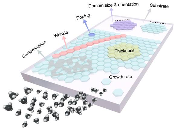
Advances in CVD Growth Techniques
Recent advancements in Chemical Vapor Deposition (CVD) techniques have significantly enhanced the quality and scalability of graphene production. These improvements are largely attributed to the exploration of diverse carbon sources, growth substrates, and optimized growth conditions. For instance, the use of copper (Cu) foils has proven effective in producing large-area monolayer graphene, which is crucial for industrial applications.
One notable development is the adoption of alternative precursor gases, such as metal-organic frameworks (MOFs) and metal-organic chemical vapor deposition (MOCVD). MOFs, known for their porous structure, offer potential in gas storage and separation, while MOCVD extends the versatility of CVD by employing metal-organic compounds as precursor gases. This innovation is particularly promising for the fabrication of advanced materials like III-V semiconductors.
Moreover, the integration of advanced control systems has revolutionized the CVD process. Feedback control systems now enable real-time monitoring and adjustment of precursor gas flow rates and reaction chamber temperatures. This dynamic control ensures the uniformity and quality of the deposited films, minimizing material waste and enhancing process efficiency. These technological leaps not only refine the current CVD methodologies but also pave the way for future innovations in graphene production.
Graphene Transfer Technology
Importance and Challenges of Graphene Transfer
The transfer of graphene from its growth substrate to a target substrate is a critical step in its application and characterization. This process is essential for leveraging graphene's unique properties in various fields, including electronics, optics, and composites. However, the transfer process presents several challenges that must be addressed to ensure the integrity and functionality of the transferred graphene.
One of the primary challenges is maintaining the structural integrity of graphene during transfer. Graphene is a delicate material that can easily be damaged by mechanical stress, leading to the formation of cracks, holes, and wrinkles. These defects not only compromise the material's performance but also hinder its integration into functional devices. Therefore, a perfect transfer should ensure the continuity of the graphene film without introducing such mechanical damage.
Another significant challenge is avoiding contamination during the transfer process. Graphene grown on metallic substrates often requires transfer to non-metallic substrates for application. However, the transfer process can introduce residues and impurities, such as metal ions or organic contaminants, which can alter the electronic properties of graphene. Ensuring that the transferred graphene remains clean and free from such contaminants is crucial for maintaining its intrinsic properties.
Several transfer methods have been developed to address these challenges, each with its own set of advantages and limitations. These methods can be broadly categorized into one-time transfer and two-time transfer techniques. In one-time transfer, graphene is directly adhered to the target substrate, while in two-time transfer, a carrier film is used to facilitate the transfer from the growth substrate to the target substrate. Additionally, transfer methods can be classified based on whether they involve dissolving the growth substrate (dissolved substrate transfer) or mechanically or electrochemically separating it (separated substrate transfer). The latter is often more cost-effective as the growth substrate can be reused.
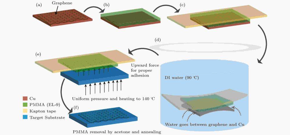
To summarize, the transfer of graphene is a pivotal step in its application, necessitating careful consideration of both structural integrity and contamination prevention. The development of reliable, stable, and low-cost transfer methods is essential for the industrialization of graphene-based technologies.
Methods and Techniques for Graphene Transfer
Graphene, grown on metallic substrates, requires meticulous transfer processes to be applied to target substrates, typically non-metallic, for practical use. The ideal transfer process should uphold three primary characteristics: maintaining the film's continuity without mechanical damage, ensuring the film remains residue-free and undoped, and being both stable and cost-effective for industrial scalability.
Several transfer methods have been developed, each with unique advantages and limitations. These methods can be broadly categorized into one-time and two-time transfer processes. In one-time transfer, graphene is directly adhered to the target substrate, while two-time transfer employs a carrier film to facilitate the movement from the growth substrate to the target substrate. Additionally, methods can be classified as dissolved substrate transfer or separated substrate transfer. Dissolved substrate transfer involves dissolving the growth substrate with an etchant to separate the graphene, whereas separated substrate transfer uses mechanical or electrochemical means to achieve separation. The latter is often more cost-effective as the substrate can be reused.
| Transfer Method | Description | Advantages | Limitations |
|---|---|---|---|
| One-Time Transfer | Direct adhesion of graphene to target substrate | Simple, straightforward | Prone to mechanical damage |
| Two-Time Transfer | Use of a carrier film to transfer graphene | Reduces mechanical stress | More complex, requires additional steps |
| Dissolved Substrate Transfer | Dissolving the growth substrate with an etchant | Effective separation | Substrate is lost, potential for residue |
| Separated Substrate Transfer | Mechanical or electrochemical separation | Substrate can be reused, cost-effective | Requires precise control to avoid damage |
These methods collectively aim to address the challenges of transferring graphene without compromising its structural integrity or introducing contaminants, thereby enabling its application in various high-tech fields.
Future Prospects and Applications of CVD Graphene
Potential Applications of CVD Graphene
CVD graphene, with its exceptional properties, is poised to revolutionize numerous industries, from electronics to biomedicine. Its potential applications span across a wide spectrum, including the development of transparent conductive films, advanced electronic devices, and flexible electronics. In the biomedical sector, CVD graphene is being explored for use in biosensors, imaging technologies, monitoring devices, and even wound dressings. Notably, its ability to enhance drugs and therapeutic treatments, particularly for cancer patients, underscores its transformative potential in healthcare.
In the realm of electronics, CVD graphene is being harnessed to design heterostructures with semiconductors and Van der Waals heterostructures based on two-dimensional materials. This innovation extends into various scientific and industrial areas such as nonvolatile memories, optoelectronics, nanomechanical systems, interconnections, bioelectronics, and thermal management. Additionally, graphene-based photodetectors, light-emitting diodes, and solar cells are emerging as promising applications due to their superior performance in transparent electrodes and active layers used in photoelectric devices.
Future research will likely focus on enhancing the quality and scalability of CVD graphene, aiming to meet the demands of large-scale industrial applications. As the technology continues to evolve, the production of graphene on larger scales and larger surface areas will become increasingly feasible, driven by advancements in CVD techniques. This evolution is expected to unlock new frontiers in both technological and industrial applications, making CVD graphene a cornerstone of future innovation.
Research Directions for CVD Graphene
Future research in the field of CVD graphene promises to unlock new frontiers in material science and technology. Key areas of focus include the advancement of techniques for producing large-area single-crystal graphene, the development of graphene ribbons with precise electronic properties, and the creation of macroscopic graphene structures with enhanced mechanical and electrical characteristics. These innovations are not only aimed at improving the scalability and quality of graphene production but also at broadening its applications across various industries.
Moreover, the exploration of low-temperature growth methods for graphene on diverse substrates is gaining traction. This approach seeks to mitigate the limitations of conventional high-temperature CVD processes, which can be prohibitive for certain substrate materials. By lowering the growth temperature, researchers hope to expand the range of compatible substrates, thereby facilitating the integration of graphene into a wider array of electronic and optoelectronic devices.
In addition to these technical advancements, the development of graphene-based heterostructures is another promising avenue. These heterostructures, which combine graphene with other two-dimensional materials, offer the potential for creating new classes of devices with unique properties. For instance, the integration of graphene with semiconductors and Van der Waals materials could lead to breakthroughs in nonvolatile memory, optoelectronics, and nanomechanical systems.
The ongoing research efforts are also driven by the need to address the commercial realities of graphene production. While CVD graphene has shown great promise as a solution for producing perfect monolayers in a cost-effective, continuous process, the journey from laboratory to industrial scale has been fraught with challenges. As the technology matures, researchers are increasingly focused on bridging this gap, ensuring that the dream of large-scale, high-quality graphene production becomes a commercial reality.
Related Products
- CVD Diamond Dressing Tools for Precision Applications
- Multi Heating Zones CVD Tube Furnace Machine Chemical Vapor Deposition Chamber System Equipment
- CVD Diamond Domes for Industrial and Scientific Applications
- CVD Diamond for Thermal Management Applications
- Chemical Vapor Deposition CVD Equipment System Chamber Slide PECVD Tube Furnace with Liquid Gasifier PECVD Machine
