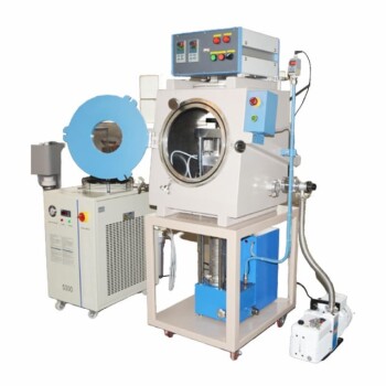
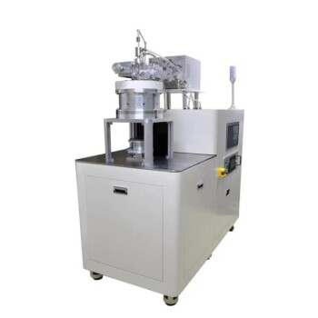
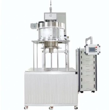
Passivation Layer Thin Film Deposition Methods
Core Process in TOPCon Cell Preparation
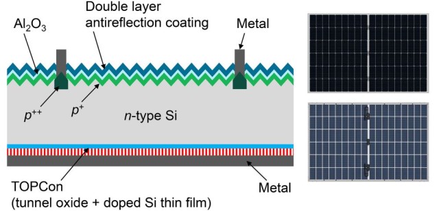
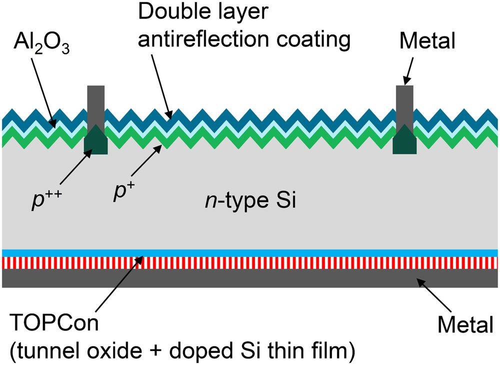
The preparation process of TOPCon cells is a meticulous sequence of steps, each critical to the overall efficiency and performance of the final product. This process begins with cleaning and fluffing, ensuring that the surface of the silicon wafer is free from contaminants that could impede subsequent steps. Following this, the front-side boron diffusion is performed to introduce boron atoms into the silicon lattice, enhancing the cell's electrical properties.
Next, the BSG removal and back-side etching are carried out to clean the back surface and prepare it for further processing. This is followed by the oxide layer passivation contact preparation, where an oxide layer is deposited to passivate the silicon surface, reducing recombination losses. The front-side alumina deposition then provides an additional layer of protection and passivation.
Subsequently, front-side and back-side silicon nitride deposition are performed using chemical vapor deposition (CVD), which is a pivotal step in the process. CVD is the core process link in this sequence, as it ensures the uniform and high-quality deposition of silicon nitride, which is crucial for the cell's passivation and anti-reflection properties. The CVD process involves the chemical reaction of gas mixtures at elevated temperatures, resulting in the deposition of a solid film on the silicon wafer.
After the deposition of silicon nitride, the process continues with screen printing to apply conductive pastes for the formation of electrical contacts. This is followed by sintering, which fuses the pastes to the silicon, creating robust electrical connections. The final steps include testing and sorting to ensure that each cell meets the required performance standards before being integrated into modules.
In summary, the TOPCon cell preparation process is a complex yet highly controlled sequence of steps, with CVD playing a central role in achieving the desired passivation and performance characteristics.
Classification by Film-Forming Method
The passivation layer thin film deposition process is categorized into two primary methods based on how the film is formed: Physical Vapor Deposition (PVD) and Chemical Vapor Deposition (CVD). Each method has its unique mechanisms and applications within the photovoltaic industry.
PVD involves the physical transportation of material from a source to the substrate, typically under vacuum conditions. This method includes techniques such as evaporation, sputtering, and ion beam deposition. PVD is known for its ability to produce high-quality, dense films with excellent adhesion to the substrate. However, it often requires more complex equipment and can be less efficient for large-scale production compared to CVD.
On the other hand, CVD relies on chemical reactions between gases to deposit a solid film onto the silicon wafer surface. This method is further divided into several subcategories based on the reaction conditions, including Atmospheric Pressure CVD (APCVD), Low-Pressure CVD (LPCVD), Plasma-Enhanced CVD (PECVD), High-Density Plasma CVD (HDPCVD), and Atomic Layer Deposition (ALD). Among these, LPCVD and PECVD are particularly prominent in the TOPCon cell manufacturing process due to their efficiency and scalability.
The prevalence of CVD in the industry is underscored by the higher percentage of CVD process equipment in use. This is largely due to CVD's ability to handle large-scale production more efficiently, its adaptability to various cell processes, and its lower operational costs compared to PVD. Despite the higher initial investment in CVD equipment, the long-term benefits in terms of production speed and cost-effectiveness make it the preferred choice for many manufacturers.
In summary, while both PVD and CVD have their respective merits, the dominance of CVD in the passivation layer thin film deposition process is a testament to its efficiency and suitability for large-scale photovoltaic production.
Physical Vapor Deposition (PVD)
Physical Vapor Deposition (PVD) is a critical process in thin film technology, involving the transformation of a material from a solid state to a vapor state and subsequent redeposition onto a substrate. This method is typically employed under low-pressure gas or plasma conditions, facilitating the formation of thin films on various substrates. The primary techniques within PVD include evaporation and sputtering, each with distinct operational mechanisms and applications.
Evaporation is a process where the source material is heated to its vaporization point in a vacuum environment. This heating causes the material to transition into a vapor, which then condenses onto the substrate, forming a thin film. This method is particularly effective for materials with low melting points and is commonly used for depositing metals and certain dielectric materials.
In contrast, sputtering involves the use of a plasma to bombard the source material with ions, typically argon ions. This ion bombardment dislodges atoms from the source material, creating a vapor that subsequently deposits onto the substrate. Sputtering is renowned for its ability to deposit a wide range of materials, including those with high melting points and complex compositions, making it a versatile choice for various industrial applications.
PVD processes are essential in the manufacturing of items that require precise and functional thin films, such as in the electronics and optics industries. The ability to control the deposition parameters, such as temperature, pressure, and plasma conditions, allows for the creation of films with specific mechanical, optical, chemical, or electronic properties. This precision makes PVD a cornerstone in the development of advanced technologies and high-performance components.
Chemical Vapor Deposition (CVD)
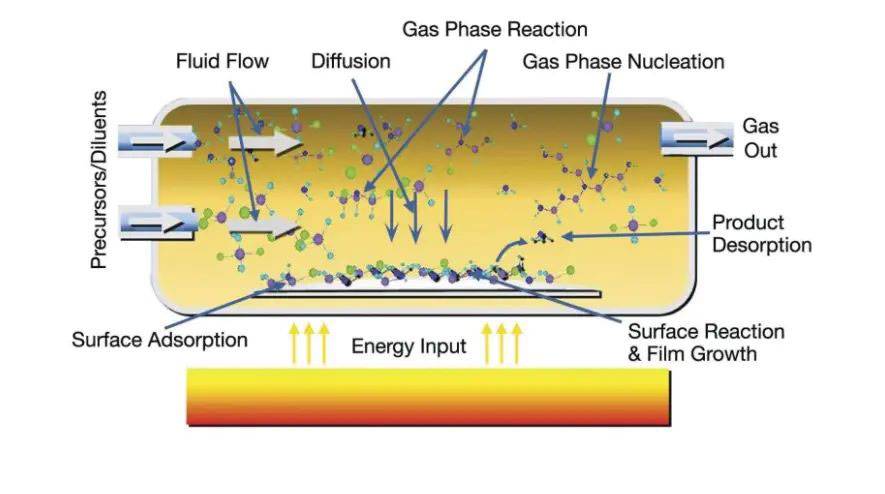
Chemical Vapor Deposition (CVD) is a sophisticated vacuum deposition method employed to produce high-quality, high-performance solid materials, often utilized in the semiconductor industry for thin film deposition. The process involves exposing a silicon wafer (substrate) to one or more volatile precursors, which undergo chemical reactions and/or decomposition on the substrate surface to form the desired film. These reactions typically yield volatile by-products that are subsequently removed by the gas flow within the reaction chamber.
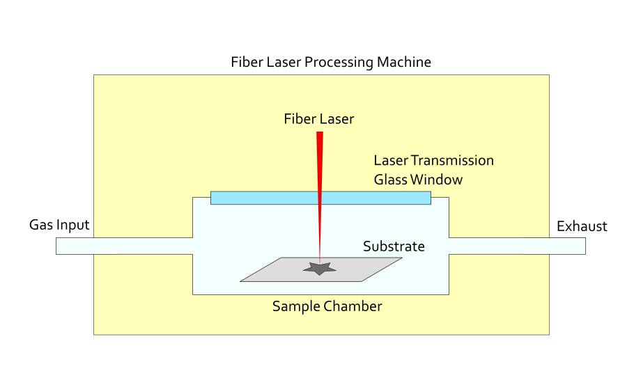
CVD techniques are broadly classified based on reaction conditions such as pressure and precursor type. This classification includes:
- Atmospheric Pressure CVD (APCVD): Conducted under atmospheric pressure.
- Low-Pressure CVD (LPCVD): Operated under reduced pressure to enhance uniformity and film quality.
- Plasma-Enhanced CVD (PECVD): Utilizes plasma to facilitate chemical reactions at lower temperatures.
- High-Density Plasma CVD (HDPCVD): Employs high-density plasma for superior film properties.
- Atomic Layer Deposition (ALD): A sequential, self-limiting process that deposits films one atomic layer at a time.
Each variant of CVD offers unique advantages and is selected based on the specific requirements of the semiconductor fabrication process, such as film uniformity, deposition rate, and temperature constraints.
CVD is not only pivotal in semiconductor manufacturing but also finds applications in microfabrication for depositing a variety of materials, including silicon dioxide, carbide, nitride, and oxynitride, as well as advanced materials like carbon nanotubes and graphene. The versatility and precision of CVD make it an indispensable technology in the realm of thin film deposition.
TOPCon Process Variants
LPCVD (Low Pressure Vapor Deposition)
LPCVD, or Low Pressure Chemical Vapor Deposition, is a sophisticated thermal process used to deposit thin films from gas-phase precursors at subatmospheric pressures. This method involves the use of one or several gaseous substances that undergo thermal decomposition reactions at low pressures. These reactions result in the formation of the desired film on the substrate surface. The process conditions are meticulously selected to ensure that the growth rate is primarily governed by the rate of the surface reaction, which is highly temperature-dependent.
The temperature control in LPCVD is executed with great precision, leading to exceptional uniformity across within-wafer, wafer-to-wafer, and run-to-run variations. This precision is crucial for maintaining consistency in the quality and properties of the deposited films. The low pressure environment in LPCVD significantly enhances the gas diffusion coefficient and the mean free path within the reaction chamber. This improvement translates to better film uniformity, resistivity uniformity, and trench coverage filling capability. The faster gas transport rate in the low-pressure environment also aids in quickly removing impurities and reaction by-products from the substrate, thereby suppressing self-doping and enhancing production efficiency.
Moreover, LPCVD does not necessitate the use of carrier gases, which substantially reduces the potential for particle contamination. This makes LPCVD a preferred method in the high-value semiconductor industry for the deposition of thin films. Recent advancements in LPCVD technology are focusing on achieving low stress and multifunctional capabilities, further expanding its applications and improving its performance in various industrial settings.
PECVD (Plasma-Enhanced Vapor Deposition)
Plasma-enhanced chemical vapor deposition (PECVD) is a sophisticated technique used to deposit thin films on substrates, particularly in the semiconductor industry. This method leverages microwave or radio frequency (RF) energy to locally generate a plasma, which significantly enhances the chemical reactions necessary for film formation. Unlike traditional CVD processes that require higher temperatures, PECVD operates at relatively lower temperatures, typically between 200 and 500°C. This temperature reduction is crucial for substrates that are sensitive to heat, such as semiconductor wafers, as it minimizes the risk of thermal damage.
The plasma generated in PECVD can be ignited directly in the vicinity of the substrate, a method known as the direct plasma technique. This proximity ensures that the reactive species are efficiently utilized, leading to high-quality film deposition. However, direct plasma exposure can pose risks to sensitive substrates due to potential radiation and ion bombardment, necessitating careful process control.
PECVD is widely employed for depositing dielectric films such as SiO₂, Si₃N₄, and SiOxNy. The process involves creating a plasma of reacting gases through RF energy, which facilitates chemical reactions within the deposition chamber. The energy required for these reactions is partly supplied by heating the substrate to a moderate temperature, typically below 350°C, and partly by the plasma itself. This dual energy source enhances the efficiency and quality of the deposited films.
The films produced by PECVD are versatile, serving various critical functions in semiconductor devices. These include acting as capacitor dielectrics, chemical passivation layers, electrical insulators, reactive ion etching masks, and optical anti-reflective coatings. Notably, PECVD systems offer advanced capabilities such as stress control, high uniformity, tunable refractive index, and the ability to produce conformal SiNₓ films, making it a preferred choice for many modern semiconductor manufacturing processes.
PEALD+PECVD (Plasma-Enhanced Atomic Layer Deposition)
PEALD+PECVD represents a synergistic approach that integrates the precision and control of Atomic Layer Deposition (ALD) with the efficiency and versatility of Plasma-Enhanced Chemical Vapor Deposition (PECVD). This hybrid technique leverages the self-limiting nature of ALD, which ensures uniform and conformal film deposition at the atomic level, while harnessing the plasma-driven chemical reactions of PECVD to accelerate the deposition process and enhance material properties.
In PECVD, the plasma environment provides the necessary energy to facilitate the chemical reactions that drive the deposition process. This plasma is typically generated using radio frequency (RF) or microwave energy, operating at pressures ranging from 2 to 10 Torr and substrate temperatures between 200 to 400°C. The low temperature operation of PECVD is particularly advantageous, allowing the use of temperature-sensitive substrates that would otherwise be compromised by higher temperatures required in other CVD techniques.
When combined with ALD, PECVD's ability to operate at lower temperatures becomes even more significant. ALD, which traditionally requires precise control of temperature and reactant pulse times, benefits from the plasma's energy input, enhancing the reactivity of the precursors and potentially reducing the overall process time. This combination results in films that are not only highly conformal but also possess superior mechanical and electrical properties.
The applications of PEALD+PECVD are vast, particularly in the semiconductor and photovoltaic industries. For instance, in the production of solar cells, this technique can be used to deposit dielectric films such as SiO2, Si3N4, and SiOxNy, which are crucial for achieving efficient passivation and anti-reflective coatings. These films are essential for improving the overall efficiency and performance of solar cells, making PEALD+PECVD a key technology in the advancement of renewable energy solutions.
Moreover, the conformal and uniform nature of films deposited via PEALD+PECVD makes them ideal for use in various microelectronic applications, including capacitor dielectrics, chemical passivation layers, electrical insulators, and reactive ion etching masks. The ability to precisely control film thickness and uniformity at the atomic level ensures that these films meet the stringent requirements of modern semiconductor devices.
In summary, PEALD+PECVD not only marries the best attributes of ALD and PECVD but also opens new avenues for innovation in thin film deposition technologies. By combining the precision of ALD with the efficiency of PECVD, this hybrid method offers a versatile and powerful tool for the next generation of semiconductor and photovoltaic devices.
PVD (Physical Vapor Deposition)
Physical Vapor Deposition (PVD) is a sophisticated technique used to deposit thin films on various substrates through physical processes under vacuum conditions. This method involves the vaporization of a solid or liquid material, which is then transported as a vapor through a controlled environment, typically a vacuum or low-pressure gaseous or plasma medium. Upon reaching the substrate, the vaporized material condenses, forming a thin film.
The material being vaporized can be an element, alloy, or compound, offering versatility in the types of films that can be created. Notably, some PVD processes enable the deposition of compound materials through reactive deposition. This involves the interaction of the depositing material with gases in the deposition environment or with co-depositing materials, such as the formation of titanium nitride (TiN) or titanium carbide (TiC).
PVD processes are renowned for their ability to produce films with thicknesses ranging from a few nanometers to thousands of nanometers. These processes are not limited to single-layer films; they can also be employed to create multilayer coatings, thick deposits, and even free-standing structures. The high purity and efficiency of PVD-deposited films make them highly desirable for a wide array of applications, often surpassing the performance of films produced by other deposition methods.
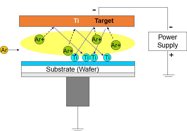
Key methods within the PVD category include Sputtering and Thermal Evaporation. In Sputtering, high-energy particles bombard a target material, causing atoms to be ejected and deposited onto the substrate. Thermal Evaporation, on the other hand, involves heating a source material until it vaporizes, with the vapor then condensing on the substrate. Both methods ensure that the material is transported and accumulated atom-by-atom or molecule-by-molecule in a vacuum, resulting in films with exceptional purity and efficiency.
Technology Comparison
LPCVD Advantages and Disadvantages
Low Pressure Chemical Vapor Deposition (LPCVD) offers several advantages, particularly in its efficiency, yield, and production capacity. One of its standout features is its strong step coverage ability, which makes it ideal for complex three-dimensional structures, ensuring good side wall coverage. This capability is crucial in the photovoltaic cell manufacturing process, especially for producing TOPCon cells. Additionally, LPCVD allows for good composition and structure control due to its ability to perform deposition at lower temperatures, which is beneficial for maintaining the chemical composition and microstructure of the film.
However, LPCVD is not without its challenges. The process requires maintaining a low-pressure environment, leading to relatively high energy consumption. The use of numerous quartz consumables in the LPCVD process also drives up operational costs. Moreover, LPCVD's deposition rate is slower compared to Plasma Enhanced Chemical Vapor Deposition (PECVD), limiting its productivity. Another significant issue is the phenomenon of bypass plating, where deposition occurs in non-target areas, affecting the consistency and quality of the final product.
Despite these drawbacks, LPCVD's high film quality, achieved through its low-pressure environment, remains a key advantage, contributing to improved uniformity and overall film quality. This balance of pros and cons makes LPCVD a critical technology in the photovoltaic industry, particularly in the intricate process of TOPCon cell production.
PECVD Advantages and Disadvantages
PECVD (Plasma-Enhanced Chemical Vapor Deposition) presents a series of advantages that make it a preferred method for various cell processes, including PERC, TOPCON, and HJT. One of its primary benefits is the high deposition rates it offers. This efficiency significantly enhances production throughput, making it a time-effective solution for large-scale manufacturing. Additionally, PECVD enables in-situ doping, which simplifies the process by allowing doping to occur concurrently with the deposition. This not only streamlines the workflow but also reduces the potential for contamination.
The low deposition temperature of PECVD is another key advantage. By utilizing polyatomic gas discharge, this technique can deposit compound films at reduced temperatures, thereby minimizing thermal damage to the substrate. This低温沉积特性 is particularly beneficial for substrates that are sensitive to high temperatures, broadening the range of materials that can be used in the process. Moreover, PECVD's high deposition efficiency is attributed to the uneven electric field distribution in front of the cathode, which concentrates chemical reactions in the cathode drop zone. This localized high-activity area accelerates the reaction speed and enhances deposition efficiency, as illustrated in the distribution of NH3 formation rate in DC-PECVD.
Despite its numerous advantages, PECVD is not without its drawbacks. One significant concern is the potential instability of the deposited films. Films formed through PECVD may exhibit issues such as film bursting, which can compromise the integrity and performance of the final product. Additionally, the complexity of PECVD equipment necessitates high maintenance and debugging efforts, adding to operational costs and complexity. There is also the risk of film quality fluctuations due to plasma instability, which can affect the uniformity and consistency of the deposited layers.
In summary, while PECVD offers significant advantages in terms of deposition rate, process simplification, and cost-effectiveness, it also presents challenges related to film stability and equipment complexity. These factors must be carefully considered when selecting PECVD for specific cell processes.
PEALD+PECVD and PVD Advantages
PEALD+PECVD and PVD each offer distinct advantages in the realm of thin film deposition, particularly in the context of photovoltaic cell manufacturing.
PEALD+PECVD excels in addressing inhomogeneity issues. By combining the precision of Atomic Layer Deposition (ALD) with the efficiency of Plasma-Enhanced Chemical Vapor Deposition (PECVD), this hybrid technique ensures uniform film thickness and composition across the substrate. This is crucial for maintaining consistent electrical properties and enhancing the overall efficiency of photovoltaic cells. The low deposition temperature of PECVD, typically below 350°C, ensures minimal thermal stress on the substrate, which is particularly beneficial for temperature-sensitive materials like plastics. Additionally, the high deposition efficiency of PECVD, facilitated by energetic particles in the plasma, further contributes to faster and more controlled film formation.
On the other hand, PVD stands out for its fast film formation and multifunctional upgrading. Unlike PECVD, which relies on chemical reactions, PVD employs physical processes such as evaporation, sputtering, or ion beam techniques to deposit material onto the substrate. This results in rapid film formation, making PVD ideal for applications requiring quick turnaround times. Moreover, PVD offers the advantage of no winding plating, ensuring that the deposited films are free from defects that could arise from mechanical stresses. The versatility of PVD also allows for multifunctional upgrades, enabling the deposition of complex, multi-layered structures with tailored properties.
However, it is worth noting that while PVD and PEALD+PECVD offer these compelling advantages, they also come with higher equipment costs. The sophisticated machinery required for these advanced deposition techniques necessitates significant investment, which may be a consideration for manufacturers balancing cost and performance.
In summary, while both PEALD+PECVD and PVD present unique advantages in thin film deposition, their selection depends on the specific requirements of the application, including considerations of film uniformity, deposition speed, and cost-effectiveness.
Related Products
- Aluminized Ceramic Evaporation Boat for Thin Film Deposition
- Tungsten Evaporation Boat for Thin Film Deposition
- Molybdenum Tungsten Tantalum Evaporation Boat for High Temperature Applications
- Electron Beam Evaporation Coating Oxygen-Free Copper Crucible and Evaporation Boat
- HFCVD Machine System Equipment for Drawing Die Nano-Diamond Coating
