Introduction to MOCVD
Definition and Overview
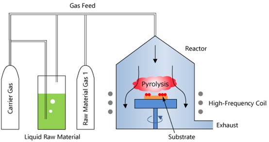
Metal Organic Chemical Vapor Deposition (MOCVD) is a sophisticated process that utilizes organic compounds of group III or II elements, along with oxides or hydrides of group V or VI elements, as the primary raw materials for crystal growth. These materials undergo vapor phase epitaxy on a substrate through a thermal decomposition reaction, resulting in the growth of a diverse array of compound semiconductors. These semiconductors belong to either the group III-V or II-VI categories, and can also form multilayered solid solutions, all of which are produced as thin-layered single-crystal materials.
The process of MOCVD is highly versatile, capable of synthesizing a wide range of semiconductor materials with precise control over their composition and structure. This makes it an indispensable tool in the semiconductor industry, where the demand for high-quality, precisely engineered materials is paramount.
Historical Development
The inception of Metal Organic Chemical Vapor Deposition (MOCVD) can be traced back to 1968, marking a pivotal moment in the realm of semiconductor technology. The technique was initially developed to produce Gallium Arsenide (GaAs) single-crystal thin films, a material crucial for various electronic and optical applications. This pioneering effort involved the utilization of organometallic compounds, specifically trimethylgallium [(CH₃)₃Ga] and arsine (AsH₃), as precursor materials. These precursors were subjected to thermal decomposition at elevated temperatures ranging from 600 to 700°C within an open-tube reactor, which was maintained under a hydrogen (H₂) atmosphere.

The historical significance of this development lies not only in the successful synthesis of GaAs thin films but also in laying the groundwork for future advancements in the field. The controlled environment of the reactor, coupled with precise temperature regulation, enabled the deposition of high-quality GaAs films, which were essential for the fabrication of early semiconductor devices. This breakthrough underscored the potential of MOCVD as a versatile and powerful method for synthesizing complex semiconductor materials, paving the way for its widespread adoption in the semiconductor industry.
Over the years, the technique has evolved significantly, incorporating advancements in precursor chemistry, reactor design, and process optimization. Today, MOCVD is recognized as a cornerstone technology in the production of a diverse array of compound semiconductors, including those from groups III-V and II-VI, as well as their multilayered solid solutions. The historical development of MOCVD thus represents a critical chapter in the ongoing narrative of semiconductor innovation, reflecting the continuous efforts to push the boundaries of material science and device fabrication.
Epitaxial Growth
Homogeneous Epitaxy
Homogeneous epitaxy is a specialized growth method where the epitaxial layer and the substrate are composed of the same material. This method is exemplified by the growth of silicon (Si) films on silicon sheets or zinc oxide (ZnO) films on ZnO substrates. The primary advantage of homogeneous epitaxy lies in its ability to achieve high lattice matching, which facilitates the production of single-crystal films with exceptional crystalline quality.
However, the pursuit of homogeneous epitaxy is not without its challenges. For certain materials, obtaining high-quality substrates that match the epitaxial layer can be exceedingly difficult. This difficulty often translates into higher costs and greater technical challenges. The stringent requirements for substrate quality necessitate advanced manufacturing techniques and rigorous quality control processes, which can significantly elevate the overall cost of the epitaxial growth process.
Despite these challenges, homogeneous epitaxy remains a critical technique in the semiconductor industry due to its ability to produce high-quality single-crystal films. The precise lattice matching achieved through this method is essential for applications where material purity and structural integrity are paramount, such as in the fabrication of advanced semiconductor devices and optical components.
Heterogeneous Epitaxy
Heterogeneous epitaxy is a critical technique in semiconductor growth, where the lattice constants of the substrate material and the epitaxial layer material must be closely matched. This matching is essential to prevent the accumulation of stress between the epitaxial layer and the substrate during the growth process, which could lead to an excessive defect density in the epitaxial layer. The mismatch in lattice constants can result in significant stress, causing defects such as dislocations and misfit dislocations, which degrade the quality of the epitaxial layer.
In addition to lattice matching, the coefficients of thermal expansion (CTE) of the substrate and the epitaxial layer must also be similar. This similarity is crucial to ensure that the epitaxial layer does not deform or detach when the temperature changes. For instance, during the cooling phase at the end of the growth process or when the subsequent device is heated, a significant difference in CTE can cause the epitaxial layer to buckle or peel off, compromising the integrity and performance of the device.
To illustrate the importance of these parameters, consider the following table:
| Parameter | Importance |
|---|---|
| Lattice Constant Match | Prevents stress accumulation, reduces defect density |
| Thermal Expansion Match | Ensures mechanical stability, prevents deformation and detachment |
By meticulously selecting materials with compatible lattice constants and thermal expansion coefficients, researchers can achieve high-quality heterogeneous epitaxy, paving the way for advanced semiconductor devices.
MOCVD Principles
Chemical Reactions
The MOCVD epitaxy process is a sophisticated physicochemical endeavor, intricately intertwined with the pyrolysis and chemosynthesis of volatile organometallic compounds and gaseous hydride reactive precursors. This process can be dissected into several key chemical reactions, each playing a pivotal role in the formation of the desired thin-film structures.
Key Reactions in MOCVD
-
Pyrolysis of Organometallic Compounds:
- Reaction Type: Thermal decomposition.
- Example: Decomposition of trimethylgallium (TMGa) at elevated temperatures to form gallium and methane.
- Equation:
(CH3)3Ga → Ga(s) + 3CH4(g)
-
Chemosynthesis of Hydride Precursors:
- Reaction Type: Hydrogenation.
- Example: Reaction of arsine (AsH3) to form arsenic and hydrogen gas.
- Equation:
AsH3(g) → As(s) + 3/2H2(g)
-
Surface Reactions:
- Reaction Type: Adsorption and surface diffusion.
- Example: Adsorption of gallium and arsenic atoms on the substrate surface, leading to the formation of a crystalline lattice.
- Process: The adsorbed atoms diffuse and combine to form a stable lattice structure.
Complexity and Control
The complexity of the MOCVD process lies in the precise control of these reactions. Factors such as temperature, pressure, and the flow rates of the precursor gases must be meticulously regulated to ensure the desired chemical reactions proceed efficiently. Any deviation can lead to the formation of defects, non-uniform layers, or even complete failure of the epitaxial growth.
Role of Catalysts
In some advanced MOCVD processes, the use of catalysts can enhance the efficiency of certain reactions. For instance, the addition of a catalyst can lower the activation energy required for the pyrolysis of organometallic compounds, thereby improving the overall yield and quality of the epitaxial layers.
By understanding these fundamental chemical reactions, researchers and engineers can better optimize the MOCVD process for the production of high-quality semiconductor materials, paving the way for advancements in various electronic and optoelectronic devices.
Thermodynamic and Kinetic Processes
In Metal Organic Chemical Vapor Deposition (MOCVD), crystal growth is fundamentally governed by two primary processes: thermodynamic and kinetic. The thermodynamic process serves as the engine that propels the epitaxial growth, providing the necessary energy and conditions for the chemical reactions to occur. This process ensures that the system remains in a state of equilibrium, where the free energy is minimized, thereby facilitating the formation of stable crystal structures.
On the other hand, the kinetic process dictates the rate at which these reactions proceed. It encompasses the various steps involved in the transport of reactants to the growth surface, the adsorption and surface diffusion of these reactants, and the subsequent incorporation into the crystal lattice. The epitaxial growth rate is thus determined by the efficiency of these kinetic steps, which can be influenced by factors such as temperature, pressure, and the concentration of reactants.
| Process Type | Role in Epitaxial Growth | Factors Influencing Process |
|---|---|---|
| Thermodynamic | Provides driving force for epitaxial growth | Temperature, pressure, chemical potential of reactants |
| Kinetic | Determines epitaxial growth rate | Temperature, reactant concentration, surface diffusion |
Understanding the interplay between these two processes is crucial for optimizing the MOCVD growth conditions to achieve high-quality epitaxial layers. By fine-tuning both thermodynamic and kinetic parameters, researchers can control the morphology, composition, and defect density of the grown crystals, thereby enhancing the performance of semiconductor devices fabricated using MOCVD technology.
MOCVD Equipment
Gas Source Transportation System
The gas delivery system in MOCVD technology is a critical component, designed to handle the precise and safe transportation of various gas sources. This system necessitates the use of highly clean, leak-free, stainless steel gas lines to ensure the integrity and purity of the gases being transported. These gas lines are responsible for conveying a diverse array of gas sources, including both material component gaseous sources and dopant sources.
To maintain the high standards required for MOCVD processes, the gas delivery system must undergo rigorous cleaning and inspection procedures. This ensures that the gas lines remain free from any contaminants that could compromise the quality of the epitaxial growth. The system's design also incorporates advanced leak detection mechanisms to prevent any unintended gas leaks, which could lead to safety hazards or process inefficiencies.
The gas sources transported by this system are integral to the MOCVD process, as they provide the necessary precursors for the chemical reactions that drive epitaxial growth. These sources include volatile organometallic compounds and gaseous hydride reactive precursors, which are essential for the formation of the desired semiconductor materials. The precise control over the delivery of these gas sources is crucial for achieving the uniformity and quality of the epitaxial layers.
In summary, the gas delivery system in MOCVD technology plays a pivotal role in ensuring the successful growth of high-quality semiconductor materials. Its meticulous design and maintenance are essential for maintaining the purity and safety of the gas sources, thereby supporting the overall efficiency and effectiveness of the MOCVD process.
Reaction Chamber
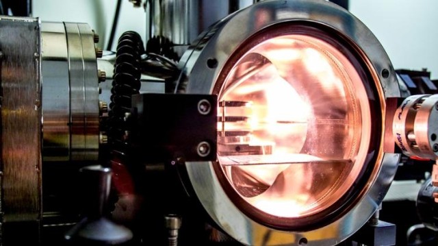
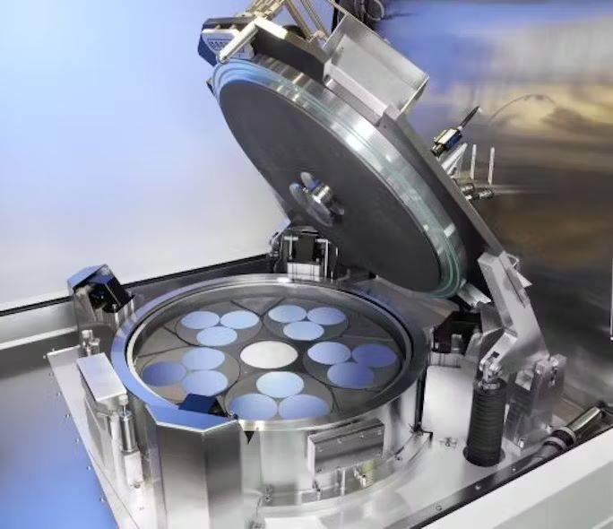
The reaction chamber in a Metal Organic Chemical Vapor Deposition (MOCVD) system is a critical component designed to facilitate the controlled growth of semiconductor layers. This chamber is typically constructed from high-purity quartz or stainless steel, materials chosen for their resistance to the corrosive gases and high temperatures involved in the process. The chamber's design includes several key elements:
- Carrier Base: This base supports the substrate and ensures uniform distribution of the gases.
- Substrate Heater: A crucial part of the setup, the heater maintains the substrate at the precise temperatures required for the chemical reactions to occur.
- Manometer: This device measures the pressure within the chamber, which is a critical parameter for controlling the growth process.
- Temperature Sensor: Embedded within the chamber, this sensor provides real-time data on the temperature, allowing for precise control.
- Cooling Water Channel: This channel circulates water to cool the chamber, preventing overheating and ensuring the stability of the growth environment.
Each of these components plays a vital role in maintaining the controlled conditions necessary for the successful deposition of high-quality semiconductor layers.
Tail Gas Treatment System
The tail gas treatment system is an indispensable component of the MOCVD process, ensuring the safe and efficient operation of the entire system. This system is always active, regardless of whether the gaseous sources are currently in use, underscoring its critical role in maintaining safety protocols. The primary function of the tail gas treatment system is to neutralize and dispose of any residual gases that could pose hazards if left untreated.
One of the key aspects of the tail gas treatment system is its ability to handle a variety of gases, including those that are toxic, corrosive, or flammable. This necessitates the use of advanced filtration and neutralization techniques to ensure that these gases are rendered harmless before being released into the environment. The system typically includes multiple stages of treatment, such as scrubbers, adsorption beds, and catalytic converters, each designed to address specific types of hazardous gases.
Moreover, the tail gas treatment system is integrated with the overall control and monitoring system of the MOCVD equipment. This integration allows for real-time monitoring of gas composition and flow rates, ensuring that any anomalies are detected and addressed promptly. The system's robust design ensures that it can withstand the high temperatures and pressures associated with the MOCVD process, maintaining its effectiveness over long periods of operation.
In summary, the tail gas treatment system is a vital safety measure in the MOCVD process, ensuring that the environment and personnel remain protected from harmful byproducts. Its continuous operation and advanced treatment capabilities make it an essential component of the MOCVD equipment setup.
Control and In-Situ Monitoring System
The control and in-situ monitoring system is a critical component of the MOCVD equipment, ensuring the precise and efficient growth of semiconductor materials. This system is primarily composed of an industrial control computer, which serves multiple essential functions during the growth process. Firstly, it is used to write and execute growth programs, which dictate the specific conditions and sequences required for optimal material growth. These programs are meticulously designed to control parameters such as temperature, gas flow rates, and pressure, ensuring that the chemical reactions proceed as intended.
In addition to programming, the control computer continuously monitors the material growth in real time. This involves recording various signals generated by the growth process, including sensor data on flow rates, pressure, and temperature. These signals are crucial for maintaining the stability and consistency of the growth environment. For instance, fluctuations in temperature can significantly impact the quality of the epitaxial layer, making precise temperature control essential.
The system also includes an alarm mechanism that triggers alerts in response to any deviations from the programmed conditions. This proactive approach allows for immediate corrective actions, minimizing potential errors and ensuring the integrity of the growth process. By continuously regulating these parameters in real time, the control and in-situ monitoring system plays a pivotal role in achieving high-quality, reproducible semiconductor growth.
Applications of MOCVD
Semiconductor Devices
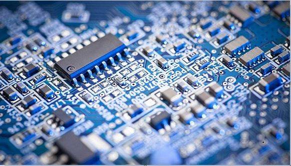
MOCVD (Metal Organic Chemical Vapor Deposition) has emerged as a pivotal technique in the fabrication of a diverse array of thin film materials, with semiconductor devices being one of its most significant applications. This method enables the precise and controlled deposition of thin layers of semiconductors, which are essential components in modern electronic and optoelectronic devices.
The versatility of MOCVD allows it to be used in the preparation of various types of semiconductor materials, each tailored to specific device requirements. For instance, it can produce high-quality epitaxial layers of III-V and II-VI compound semiconductors, such as GaAs, InP, and ZnO, which are crucial for advanced electronic components like transistors, diodes, and photovoltaic cells. Additionally, MOCVD is instrumental in the growth of multilayered structures, including quantum wells and superlattices, which are fundamental to the operation of high-efficiency LEDs and laser diodes.
Moreover, MOCVD's ability to incorporate dopants during the growth process allows for the creation of semiconductors with tailored electrical properties, essential for optimizing device performance. This capability extends to the fabrication of gas-sensitive elements, superconducting thin films, and dielectric films, further broadening its application spectrum.
In essence, MOCVD's precision, flexibility, and scalability make it an indispensable tool in the semiconductor industry, driving the innovation and advancement of electronic and optoelectronic technologies.
Heteroepitaxy
Heteroepitaxy has been successfully demonstrated on various substrates, including sapphire (Al₂O₃), spinel (MgAl₂O₄), and beryllium oxide (BeO), with the growth of GaAs being a notable early achievement. This technique has since expanded to encompass a broader spectrum of III-V compound semiconductors, such as AlAs, AlGaAs, InP, InAlAs, AlN, GaN, and GaP. The success of heteroepitaxy hinges on the careful selection of substrates that minimize lattice mismatch and thermal expansion coefficient differences, thereby reducing the defect density and ensuring the structural integrity of the epitaxial layers.
The process of heteroepitaxy is particularly challenging due to the inherent differences between the substrate and the epitaxial material. For instance, the lattice constants of the substrate and the epitaxial layer must be closely matched to prevent the accumulation of stress, which can lead to defects such as misfit dislocations. Additionally, the thermal expansion coefficients of the materials should be similar to avoid issues during thermal cycling, where the epitaxial layer may deform or even delaminate.
Despite these challenges, heteroepitaxy offers significant advantages in the fabrication of advanced semiconductor devices. By enabling the growth of materials with different properties on a single substrate, it allows for the creation of complex heterostructures that can be tailored for specific applications, such as high-speed electronics, optoelectronics, and quantum devices. The continued development of heteroepitaxy techniques is thus pivotal in pushing the boundaries of semiconductor technology.
Related Products
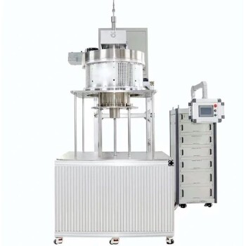
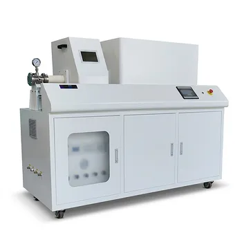
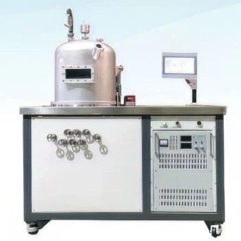
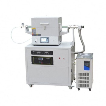
- Inclined Rotary Plasma Enhanced Chemical Vapor Deposition PECVD Equipment Tube Furnace Machine
- Microwave Plasma Chemical Vapor Deposition MPCVD Machine System Reactor for Lab and Diamond Growth
- Cylindrical Resonator MPCVD Machine System Reactor for Microwave Plasma Chemical Vapor Deposition and Lab Diamond Growth
- 915MHz MPCVD Diamond Machine Microwave Plasma Chemical Vapor Deposition System Reactor
- RF PECVD System Radio Frequency Plasma-Enhanced Chemical Vapor Deposition RF PECVD
