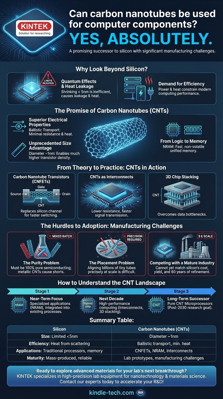
Yes, absolutely. Carbon nanotubes (CNTs) are not just a theoretical possibility for computer components; they are actively being used to build functional processors and memory in research labs. While they represent a promising successor to silicon, significant manufacturing challenges prevent their widespread commercial use today.
Carbon nanotubes offer a path beyond the physical limits of silicon, promising smaller, faster, and more energy-efficient computer components. However, the core challenge lies in shifting from lab-scale prototypes to mass-producing trillions of perfectly pure and aligned nanotubes with the same reliability as the current silicon industry.

Why Look Beyond Silicon?
For decades, the story of computing has been the story of silicon. The relentless shrinking of silicon transistors, a trend known as Moore's Law, has fueled exponential growth in computing power. But we are now approaching fundamental physical limits.
The Limits of Silicon Transistors
As silicon transistors shrink below 5 nanometers, quantum effects become a major problem. Electrons can "tunnel" through the transistor's gate even when it's off, causing leakage and generating excess heat. This makes further shrinking inefficient and unreliable.
The Demand for Unprecedented Efficiency
Modern computing, from massive data centers to mobile devices, is constrained by power consumption and heat dissipation. The energy required to move data and perform calculations is a primary bottleneck, and the heat generated limits processing density and speed.
The Promise of Carbon Nanotubes (CNTs)
CNTs are hollow cylinders of carbon atoms, essentially a sheet of graphene rolled into a tube. Their unique structure gives them extraordinary electrical and physical properties that make them an ideal candidate to replace silicon.
Superior Electrical Properties
Unlike silicon, where electrons scatter and generate heat, electrons can flow through certain CNTs with almost no resistance, a phenomenon called ballistic transport. This means CNT-based transistors could be significantly more energy-efficient, switching on and off with less power and generating far less waste heat.
Unprecedented Size Advantage
A carbon nanotube is incredibly thin, with a diameter of about one nanometer. This is significantly smaller than the channels in even the most advanced silicon transistors, opening a path to dramatically increase the density of transistors on a chip.
From Logic to Memory
The application of CNTs is not limited to processors. A technology called NRAM (Nano-RAM) uses CNTs as non-volatile memory elements. This combines the speed of DRAM with the permanence of flash storage, offering the potential for "instant-on" computers with unified memory and storage.
From Theory to Practice: CNTs in Action
Researchers have already demonstrated the viability of CNTs by building functional computer components, proving the technology works in practice, not just in theory.
Carbon Nanotube Transistors (CNFETs)
A Carbon Nanotube Field-Effect Transistor, or CNFET, replaces the silicon channel of a traditional transistor with a semiconducting CNT. By applying a voltage to a nearby gate, the flow of electrons through the tube can be switched on or off, creating a digital 1 or 0. Recent breakthroughs have even produced 3D CNFETs, stacking memory and logic to overcome data transfer bottlenecks.
CNTs as Interconnects
Even in conventional silicon chips, a significant amount of energy is lost and delay is introduced in the tiny copper wires (interconnects) that connect transistors. CNTs are being explored as a superior replacement for these interconnects, promising lower resistance and faster signal transmission between components.
Understanding the Trade-offs: The Hurdles to Adoption
Despite their immense potential, CNTs are not yet in your laptop or smartphone. The challenges are not in the fundamental physics but in the immense difficulty of manufacturing.
The Purity Problem
CNTs can be either semiconducting (acting like a switch) or metallic (acting like a wire), depending on their atomic arrangement. A batch of synthesized CNTs contains a mix of both. Even a tiny fraction of metallic CNTs in a transistor can create a short circuit, rendering the device useless. Achieving near-100% purity is the single biggest obstacle.
The Placement Problem
Modern processors contain billions or even trillions of transistors. Manufacturing a CNT-based processor requires placing these tiny tubes in precise locations and orientations across a silicon wafer. Developing a process to do this reliably and at massive scale is an enormous engineering challenge.
Competing with a Mature Industry
The global silicon fabrication industry is the most advanced and expensive manufacturing endeavor in human history, refined over 60 years. Any new technology must not only be better but also economically viable. CNT manufacturing is still in its infancy and cannot yet compete on the cost, scale, and near-perfect yield of silicon foundries.
How to Understand the CNT Landscape
The development of carbon nanotube computing is best viewed as a long-term strategic investment in the future of technology, with different applications maturing on different timelines.
- If your primary focus is near-term commercial products: Look to specialized applications like NRAM, which can be integrated into existing silicon processes more easily than full processors.
- If your primary focus is the next decade of high-performance computing: Follow research on CNTs as interconnects or in 3D chip-stacking, as these hybrid silicon-CNT approaches may offer the first performance breakthroughs.
- If your primary focus is the long-term successor to silicon: The development of a pure CNT-based microprocessor is the ultimate goal, but it remains a subject of intense academic and industrial research for the post-2030 era.
Carbon nanotubes represent a credible and powerful path forward, ensuring that the engine of technological progress continues long after silicon has reached its physical end.
Summary Table:
| Aspect | Silicon | Carbon Nanotubes (CNTs) |
|---|---|---|
| Size | Limited by quantum effects below 5nm | Diameter ~1nm, enabling higher density |
| Efficiency | Electron scattering causes heat | Ballistic transport for minimal energy loss |
| Applications | Traditional processors, memory | CNFETs, NRAM, interconnects, 3D stacking |
| Maturity | Mass-produced, highly reliable | Lab-scale prototypes, manufacturing challenges |
Ready to explore advanced materials for your lab's next breakthrough? KINTEK specializes in high-precision lab equipment and consumables, providing the tools needed for cutting-edge research in nanotechnology, materials science, and beyond. Whether you're developing carbon nanotube-based components or optimizing semiconductor processes, our solutions support innovation at every stage. Contact our experts today to discover how we can accelerate your R&D!
Visual Guide
Related Products
- Carbon Graphite Boat -Laboratory Tube Furnace with Cover
- Boron Nitride (BN) Ceramic Tube
- Hexagonal Boron Nitride HBN Thermocouple Protection Tube
People Also Ask
- What is the disadvantage of graphite furnace? Managing Reactivity and Contamination Risks
- Why is graphite used in furnaces? For Extreme Heat, Purity, and Efficiency
- What is the use of graphite tube? Essential for Extreme Heat & Corrosive Environments
- What is the use of graphite furnace? Achieve Extreme-Temperature Processing for Advanced Materials
- What is the temperature range of graphite crucible? Choose the Right Crucible for Your High-Temp Application