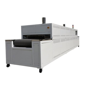
Industrial-grade open-tube diffusion furnaces improve the electrical quality of multicrystalline silicon wafers by facilitating a thermal process known as phosphorus gettering. By providing a precisely controlled high-temperature environment, the furnace allows phosphorus atoms to diffuse into the wafer surface, creating a highly doped layer that "pulls" and traps harmful transition metal impurities—such as iron and chromium—away from the wafer's interior. This process significantly reduces bulk impurity concentrations, leading to a marked increase in carrier lifetime and overall cell efficiency.
Phosphorus gettering in an open-tube furnace leverages high-temperature thermal diffusion to sequester bulk impurities at the surface. By reducing the concentration of heavy metals within the silicon, the furnace transforms the electrical properties of the wafer, enabling higher performance in the final semiconductor or solar device.
The Mechanics of Thermal Diffusion
Precision High-Temperature Control
The open-tube furnace is designed to maintain a stable, uniform temperature profile across a large batch of wafers. This consistency is vital for ensuring that phosphorus atoms penetrate the silicon crystal lattice at a predictable rate and depth.
Without this thermal stability, the resulting diffusion layer would be non-uniform, leading to localized electrical defects. The furnace acts as the engine that drives the chemical kinetics required for the gettering process to begin.
Formation of the Phosphorus Emitter
During the process, phosphorus atoms diffuse into the multicrystalline silicon surface to form an n-type emitter layer. This layer serves a dual purpose: it creates the necessary p-n junction for the device and acts as a chemical "sink."
The high concentration of phosphorus in this surface layer creates a favorable environment for mobile impurity atoms to accumulate. This "emitter formation" is the foundational step in cleaning the internal structure of the silicon.
The Impact on Impurity Migration
Trapping Transition Metals
Multicrystalline silicon often contains "bulk" impurities like chromium (Cr), manganese (Mn), and iron (Fe). These metals are detrimental to electrical performance because they act as recombination centers for charge carriers.
The highly doped phosphorus layer induces these transition metals to migrate from the interior of the wafer toward the surface. Once they reach the phosphorus-rich zone, they are effectively trapped, or "gettered," preventing them from interfering with the wafer's core electrical flow.
Reducing Bulk Metal Concentration
By moving impurities to the surface, the furnace effectively purifies the "bulk" or interior of the silicon wafer. This reduction in heavy metal concentration is essential for multicrystalline materials, which naturally have more defects than monocrystalline structures.
The primary result of this purification is a significant increase in carrier lifetime. When charge carriers can move through the silicon without being trapped by metal impurities, the electrical quality of the wafer improves drastically.
Understanding the Trade-offs
Balancing Doping Concentration
While a high concentration of phosphorus is necessary to trap impurities, excessive doping can create a "dead layer" at the surface. This layer can increase recombination at the surface, potentially offsetting the gains made by cleaning the bulk material.
Managing Thermal Budgets
The duration and temperature of the furnace cycle must be carefully managed to ensure maximum impurity migration without causing structural damage. Extended high-temperature exposure can sometimes cause other defects in multicrystalline silicon to become more active, requiring a precise balance of time and heat.
How to Apply This to Your Process
Optimization Based on Wafer Quality
The gettering profile should be tailored to the specific grade and impurity profile of your starting multicrystalline material. Different impurity types may require different temperature ramps to achieve optimal migration.
- If your primary focus is maximizing carrier lifetime: Prioritize a longer, lower-temperature gettering tail to allow slower-moving transition metals like iron to reach the phosphorus sink.
- If your primary focus is high-throughput production: Focus on optimizing the initial high-temperature diffusion phase to form the emitter quickly while maintaining sufficient gettering capacity.
- If your primary focus is reducing surface recombination: Ensure the phosphorus surface concentration is strictly controlled to prevent the formation of an electrically inactive "dead layer."
The industrial-grade open-tube furnace remains a cornerstone of silicon processing by turning a necessary doping step into a powerful purification tool.
Summary Table:
| Process Phase | Key Mechanism | Quality Impact |
|---|---|---|
| Thermal Diffusion | Precise high-temp stability | Ensures uniform phosphorus penetration |
| Emitter Formation | Phosphorus "sink" creation | Traps transition metals (Fe, Cr, Mn) |
| Impurity Migration | Bulk-to-surface transport | Drastically reduces bulk impurity concentration |
| Gettering Tail | Optimized cooling/soak | Maximizes carrier lifetime and cell efficiency |
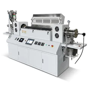
Elevate Your Semiconductor Processing with KINTEK Precision
Maximize your wafer efficiency and material purity with KINTEK’s advanced industrial-grade furnaces. From specialized open-tube and vacuum furnaces for phosphorus gettering to cutting-edge CVD, PECVD, and MPCVD systems, we provide the thermal precision required for superior semiconductor and solar cell production.
Beyond heating solutions, KINTEK offers a comprehensive laboratory portfolio, including:
- High-temperature high-pressure reactors and autoclaves
- Crushing, milling, and sieving systems for material preparation
- Hydraulic presses (pellet, hot, isostatic) for precise sample forming
- Battery research tools and essential consumables like PTFE and ceramics
Ready to optimize your thermal budget and boost carrier lifetime? Contact our technical experts today to find the perfect equipment solution tailored to your production needs.
References
- Djoudi Bouhafs, Baya Palahouane. Improvement of charge carrier lifetime in heat exchange method multicrystalline silicon wafers by extended phosphorous gettering process. DOI: 10.54966/jreen.v14i4.289
This article is also based on technical information from Kintek Solution Knowledge Base .
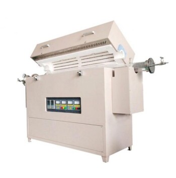
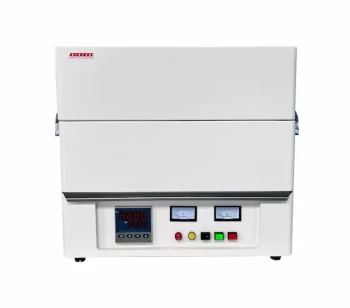
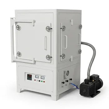
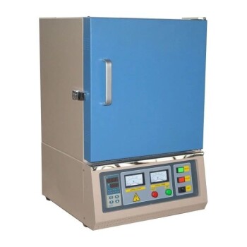
Related Products
- Vertical Laboratory Tube Furnace
- Laboratory High Pressure Vacuum Tube Furnace
- 1700℃ Laboratory High Temperature Tube Furnace with Alumina Tube
- Multi-zone Laboratory Tube Furnace
- Rotary Tube Furnace Split Multi Heating Zone Rotating Tube Furnace
People Also Ask
- How does a laboratory tube furnace provide precise temperature control? Expert Simulation for Steam Cracking
- How does a laboratory tube furnace contribute to the synthesis of RuO2 catalysts? Master Thermal Precision.
- How does a laboratory tube furnace contribute to the phase transition of antimony trioxide? Optimize Alpha-to-Beta Shift
- How does a vertical furnace work? Achieve Superior Uniformity in Semiconductor Manufacturing
- How does tube furnace temperature precision affect HEA oxidation tests? Achieve Reliable Research Results