While there is no single, definitive number, material deposition techniques are broadly organized into two fundamental categories: those that use a physical mechanism and those driven by a chemical reaction. The specific methods within each category are numerous and constantly evolving, but understanding this primary distinction is the key to navigating the field.
The critical insight is not to memorize an exhaustive list, but to grasp the fundamental difference between Physical Vapor Deposition (PVD), which physically transports a material, and Chemical Deposition, which synthesizes a material directly on a surface.

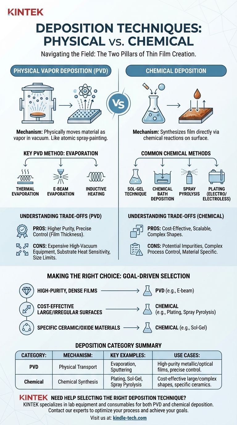
The Two Pillars of Deposition: Physical vs. Chemical
Every technique for creating a thin film or coating falls into one of two major families. The choice between them depends entirely on the desired material, the substrate it will be applied to, and the required properties of the final film.
Physical Vapor Deposition (PVD)
PVD techniques involve processes that physically move atoms or molecules from a source material onto a substrate, typically within a vacuum environment. This is like spray-painting, but on an atomic scale.
The material starts as a solid, is converted into a vapor, travels across a chamber, and then condenses back into a solid thin film on the target surface.
A Key PVD Method: Evaporation
Evaporation is a primary method within PVD where a source material is heated until its atoms vaporize and travel to coat a substrate.
There are several ways to generate this heat:
- Thermal Evaporation: Uses a resistive heat source (like the filament in a light bulb) to heat and evaporate the material.
- Electron-Beam Evaporation: Employs a high-energy, focused beam of electrons to melt and vaporize the source material, allowing for the deposition of materials with very high melting points.
- Inductive Heating: Uses radio frequency (RF) power running through a coil to induce eddy currents in a crucible, which then heats the material inside.
Chemical Deposition
In contrast to PVD, chemical deposition techniques use chemical reactions to synthesize the film directly on the substrate's surface. Precursor materials, often gases or liquids, react under specific conditions (like heat or pressure) to form a new, solid material that bonds to the surface.
This is less like painting and more like causing rust to form in a very controlled way.
Common Chemical Methods
The chemical deposition family is vast and includes a wide range of processes suited for different materials and applications.
Examples include:
- Sol-Gel Technique: Creates a solid from a chemical solution, often used for fabricating ceramic or glass coatings.
- Chemical Bath Deposition: Involves immersing the substrate in a solution where a chemical reaction slowly forms a film on its surface.
- Spray Pyrolysis: A precursor solution is sprayed onto a heated substrate, where it decomposes and forms the desired film.
- Plating: Uses a liquid solution to deposit a metallic coating, either through an electric current (electroplating) or an autocatalytic chemical reaction (electroless deposition).
Understanding the Trade-offs
Neither category is universally superior; they are chosen to solve different engineering problems. The trade-offs often center on purity, cost, and material compatibility.
Process Control and Purity
PVD processes, especially those in a high vacuum like electron-beam evaporation, generally offer higher purity and more precise control over film thickness.
Chemical deposition can sometimes introduce impurities from precursor materials or byproducts from the reaction, requiring more complex process control.
Cost and Scalability
Many chemical methods, such as spray pyrolysis or plating, can be significantly more cost-effective and easier to scale for coating large or complex-shaped areas.
PVD techniques often require expensive high-vacuum equipment, which can limit the size and throughput of the process.
Substrate and Material Limitations
PVD is highly versatile and can deposit a wide range of metals and ceramics. However, the high temperatures sometimes required can damage sensitive substrates like plastics.
Chemical methods are highly specific; the process is designed around the particular chemistry of the precursors and the desired final material.
Making the Right Choice for Your Goal
Selecting the correct deposition technique begins with clearly defining your project's primary objective.
- If your primary focus is creating high-purity, dense metallic or optical films: PVD methods like thermal or e-beam evaporation are the standard choice.
- If your primary focus is cost-effective coating of large or irregularly shaped surfaces: Chemical methods like plating or spray pyrolysis are often more practical.
- If your primary focus is fabricating specific ceramic or oxide materials from liquid precursors: Chemical routes like the sol-gel technique or chemical bath deposition are designed for this.
Ultimately, understanding the core principles of physical versus chemical pathways empowers you to select the most effective tool for the job.
Summary Table:
| Deposition Category | Core Mechanism | Key Examples | Typical Use Cases |
|---|---|---|---|
| Physical Vapor Deposition (PVD) | Physically transports material as a vapor to the substrate. | Evaporation (Thermal, E-beam), Sputtering | High-purity metallic/optical films, precise thickness control. |
| Chemical Deposition | Uses chemical reactions to synthesize the film on the substrate. | Plating, Sol-Gel, Spray Pyrolysis | Cost-effective coating of large/complex shapes, specific ceramics/oxides. |
Need help selecting the right deposition technique for your specific material and substrate?
KINTEK specializes in lab equipment and consumables, providing the right tools for both PVD and chemical deposition processes. Our experts can help you achieve high-purity coatings or cost-effective large-scale solutions.
Contact our team today to discuss your project requirements and optimize your deposition process!
Visual Guide